This thread has been locked.

If you have a related question, please click the "Ask a related question" button in the top right corner. The newly created question will be automatically linked to this question.

ADS8556: Hardware Mode, Parallel Interface, Feels like shift in values

Part Number: ADS8556

Tool/software:

I am using ads8556 and reading 6 channels in parallel mode.

>Timer starts the conversion with convst_A_B_C rising edge
>Wait for busy falling edge
>RD is toggled using a timer
>Data is copied from another pin being toggle in sync with RD and that pin being used as event for dma to copy data.

I get the conversion okay but i also get data shift in sequence and my converter falsely triggers of error. It is cause of noise? My MCU pin that sees rising/falling event and copies bus to memory might seeing glitch? or Is there something wrong with adc reading.

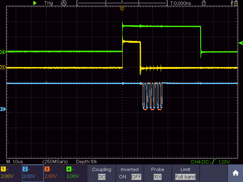
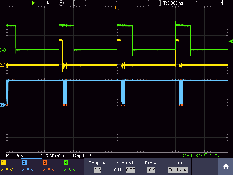
Signal coloring:
Green: Convst_A_B_C
Yellow: BUSY
Blue: RD

Orange: Toggle signal to read bus

  • I am attaching file, captured how data shifts and overlaps, Happens randomnly, and each false value i have saved in a file for you guys to see. For reference the true seq should look like this;
    197 145 13281 13077 9794 -36

    153 153 195 153 13267 13095
    13085 9755 -11 196 149 13273
    9757 -22 193 144 13274 13081
    9755 -21 196 145 13281 13058
    13075 9758 -16 189 144 13278
    154 154 198 155 13269 13096
    13076 9764 -14 193 147 13276
    13085 9773 -12 192 148 13277
    9775 -14 197 145 13279 13083
    13084 9774 -12 194 150 13275
    9777 -16 195 150 13285 13078
    13084 9778 -14 189 145 13279
    9781 -13 192 143 13279 13089
    148 148 203 149 13267 13102
    197 156 13273 13273 13273 13273
    13273 13273 13273 183 162 13259
    13081 9780 -15 185 147 13282
    13081 9785 -13 192 148 13280
    13079 9781 -17 196 144 13283
    -19 190 148 13284 13076 9783
    13093 9784 -12 190 154 13279
    13079 9785 -15 189 151 13282
    13083 9785 -18 194 139 13285
    9787 -16 197 140 13283 13080
    9786 -15 193 145 13280 13080
                                                              

  • One thing that comes to my mind is if the adc is being triggered falsely? False rising edge/noise of convst?

  • Hi Zain,

    Thanks for your question. 

    Could you share your ADC schematic so I can check if the connections are all correct? Your signals do not seem very noisy, so I do not think the CONVST signal is triggering unintentional conversions. You may add small (~33ohm) resistors on the digital signals to reduce the overshoot/ringing you are seeing. 

    It also looks like the blue RD signal is toggling before the orange signal is done reading the bus. I am wondering if this is causing the issue. Can you better align the blue and orange signals? Better yet, can you use the blue RD signal directly to trigger the DMA SPI read? This will reduce the delay.

    Best regards,

    Samiha

  • Hi, I hope you doing okay, you did reply to my previous question too, so thank you for replying.

    I am using 22R resistor in series to get rid of ringing.

    RD signal goes low and datasheet states to wait for 20ns to get stable channel reading. After that time Orange is toggle and reads the bus and it happens every time RD goes low. It is done intentionally to get stable parallel reading.

    Can you tell me what happens when, I give rising edge and doesn't read the bus?
    Shift can be cause of two reasons, bad RD toggle shifting the channel reading or noise in orange toggle which triggers dma reading and increments the memory buffer that stores readings.

    This is to be mentioned here that this shift likely happens when my converter starts i.e. there is emi noise around or switching noise. 

  • Hi Zain,

    Could you try slowing down your clock, and consequently, the ADC data rate? Let's see if this reduces the overlap. 

    Could you also try applying a DC signal to all channels so we can see if the output data holds steady?

    Best regards,

    Samiha

  • Okay, lets just put it this way, Tell me the best possible practice to use ads8556 with a MCU.

  • Hi Zain,

    That is a pretty broad question. If I were to interface ADS8556 with an MCU, I would connect:

    • the CONVST pins, together, to 1 EPWM pin
    • the DB output pins and /CS, BUSY, /RD pins to GPIO pins

    A rough example of parallel, hardware mode use would be:

    1. Give a CONVT pulse
    2. On BUSY falling edge, hold /CS low to enable parallel interface and trigger /RD low pulse to output CHA0 data on DB pins.
    3. Give /RD low pulses to read the other channels

    Best regards,

    Samiha

  • Hi Samiha,
    That solution will take a lot of mcu cycles. Considering its part of interleaved dc dc converter. I was looking for more non blocking solution. But in general I do understand what you meant.