This thread has been locked.

If you have a related question, please click the "Ask a related question" button in the top right corner. The newly created question will be automatically linked to this question.

Dual ADS1259 noise specs(?) and other stuff

Other Parts Discussed in Thread: ADS1259

Hi:

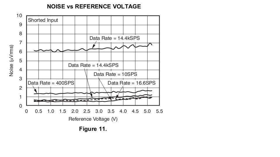
1.  I have attached the following graphic from the ADS1259 datasheet tat shows it has 2 noise specs (~ 1uVrms and 6uVrms) for the 14.4Kbps datarate. Is this correct or a typo?

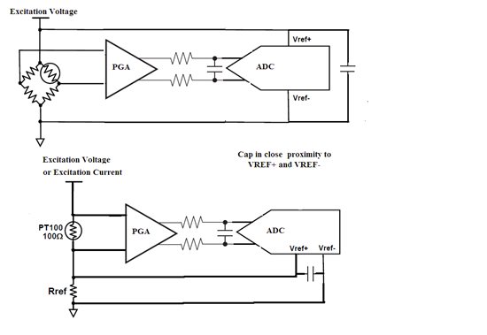
2.  Also, how do i configure the ADC for use in a ratio-metric application as this is the most precise mode of operation for all output data rates?

3.  When is the appropriate time to de-assert the START pin low? Is it after /DRDY is low or some other time?

4.  Is there a way one can simulate the ADS1259 converter? If not, what is the closest ADC one could use in Spice for simulation?

Thanks,

David

  • Hello David,

    The correct noise specs can be found on the Table 1 page 13.  Using a Data Rate of 14400 SPS and 2.5V reference, the correct input referred noise is 6.2uV RMS.  On Figure 11 on your post above, the 14,4 kSPS top label is correct; showing ~6.2 uV RMS; the bottom 14.4kSPS label is a typo.  It should read Data Rate=60 SPS, showing noise of ~0.7uV RMS.  Thank you for the feedback.

    Depending on the sensor type that is generating the input signal for the analog to digital converter, the device may be set up on a ratiometric configuration, where the source used for excitation for the sensor is also is used to generate the reference voltage.  The benefit of using a ratiometric measurement is that the drift and some of the noise of the excitation source is seen both at the input signal path and the reference signal path of the Analog to digital converter.  In this manner, the errors due to temperature drift of the excitation source and some of the noise of the excitation tends to cancel.  Two typical block diagrams are shown below.  The designer must account for the allowed differential and common mode voltage range of the PGA amplifier and the valid input voltage range of the ADC VREF inputs. In the case where RREF reference resistor is used to generate the reference voltage; the reference resistor must be in close proximity to the VREF inputs and must be a low drift, high precision resistor. 

    The START pin may be taken low before or after DRDY goes low. Please refer to the START pin timing requirements shown on Table 7 and Figure 50, 51 and 52 on the datasheet for the following: 

    --If using the device in Pulse Control Mode, the START pin is taken high and the device performs a single conversion.  The START pulse minimum width is 4 oscillator clock cycles. The DRDY remains high during the conversion.  If the START pin is taken high again during the conversion, the conversion is restarted. If the START pin is reasserted high within 22 oscillator clock cycles of the DRDY falling edge, the DRDY falls soon after and the conversion result should be discarded.   

    --If using the device in Gate control mode, the START pin is taken high and the device performs conversions continuously until the START pin is taken low.   The START pulse minimum width is 4 oscillator clock cycles.  The START pin low  to DRDY set up time to halt further conversions is 16 oscillator clock cycles (tSDSU); the START pin low hold time to complete the current conversion (in gate control mode) is also 16 oscillator clocks (tDSHD). 

    Unfortunately, there are no simulation models available for the ADS1259.

    Thank you and Regards,

    Luis