ADS1231: Deviation in offset for microvolt input in ADS1231 for strain gauge measurement.

Part Number: ADS1231

Tool/software:

Hi keith,

My customer has executed your suggested changes,  applying the 24→32 sign-extension approach you recommended produced an improvement in their results.

Below is a comparison table showing the TINA simulated voltages, the previously decoded voltages (when the 24-bit ADC result was misinterpreted)
The new voltages (with proper two’s-complement sign extension). It includes deviations (calculated − TINA) so you can see the change.

st= ADS1231_ReadRawData(&pins,&adcdata_out,500,1000);

Sl.No

Resistor network

TINA (µV)

Prev counts (type)

Prev volts (µV)

Prev deviation (µV)

New counts (type)

New volts (µV)

New deviation (µV)

1

820k / 10 Ω / 200k

88.2

50,634 (uint32_t)

77.773824

−10.426176

53,702 (int32_t)

82.486272

−5.713728

2

820k / 6.8 Ω / 200k

60

30,840 (uint32_t)

47.37024

−12.629760

34,183 (int32_t)

52.505088

−7.494912

3

820k / 1 Ω / 200k

8.8

4,294,965,869 (uint32_t)

6,597,067.57

6,597,058.77

1,365 (int32_t)

2.09664

−6.703360

4

820k / 18 Ω / 200k

158.82

98,376 (uint32_t)

151.105536

−7.714464

100,870 (int32_t)

154.93632

The least significant bit (LSB) has more full conversions of fully settled input and has weight of (0.5*3.3)/128/(2^23 - 1) = 1.536nV: For Vref = 3.3V


Short analysis:

They still see small residual deviations on the order of a few µV.
Could you please share your view on whether these are most likely tied to the ADS1231’s offset (~10 µV), resistor tolerances, or wiring/grounding influences?

Or
Do you believe these would normally be resolved once a proper system-level offset and gain calibration is performed?

And also could u please review their full code, read/conversion flow and advise/provide reference routines for the following?

  1. Read / conversion routine
  • Best-practice ADS1231 read routine.
  1. Safe method for 24→32 sign-extension
  • Confirmation of the canonical approach and any corner cases to watch for.
  1. Tare handling
  • Recommended method to capture/store tare counts (averaging method, persistence if needed, atomic update to avoid races).
  1. Factory calibration (offset & gain/span)

Please Suggested production calibration flow to correct offset (~10 µV) and gain error (one-point or two-point), recommended number of averages, resistor tolerance recommendations, and kindly share the example code for all above and applying calibration constants in firmware.

  • Hello Sarthak,

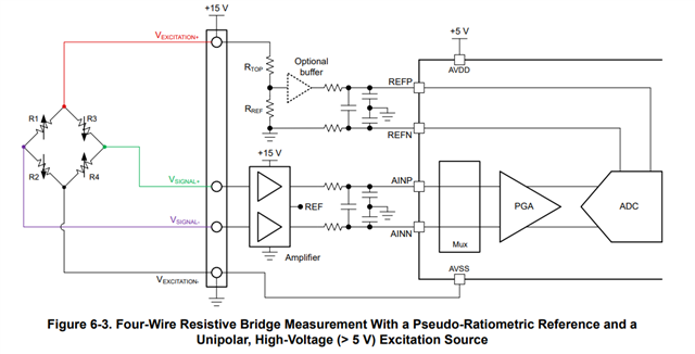
    An offset calibration (system level, 0 weight) and gain (calibration weight) will correct for much of the error.  However, the customer should consider using the same supply voltage for the bridge (resistor network) as well as the ADC reference input, or 5V.  This will allow for a ratio-metric measurement, and have much higher accuracy than possible using 9V for the bridge, and 5V for the ADC (the ADC does not support greater than 5.5V).

    The calibration procedure, and ratiometric measurements, are discussed in detail in the below application note:

    A Basic Guide to Bridge Measurements (Rev. A)

    Section 5.5 discusses calibration, and section 3.1 discusses ratiometric measurements.

    If the customer must use a bridge voltage greater than 5V (9V in the example), then I suggest using the below approach, but the system accuracy will depend on the resistor divider stability as well as the offset drift of the buffer amplifier.  Since the system will be factory calibrated, the resistor tolerance can be 0.1% and capacitor tolerance of 1% will work well.  Temperature drift will be the key concern, both for the amplifier offset voltage and the resistor divider ratio.

    Regarding averaging, the more averaging, the lower noise readings, but this will make settling time longer.  It will depend on how fast a stable reading is needed.  Using the 10sps setting of the ADC already provides for low noise measurements, but you can further lower the noise by averaging these readings in the system processor.  For factory calibration, you can average as many readings as needed to reduce noise since settling time is not as much of a concern.  For Tare, similar to factory calibration, you can average more readings since this is a customer 'initialization' of the weigh scale.  However, average 10 samples at 10sps will require 1 second, which may or may not be acceptable for the end application.  The customer will need to determine these requirements.

    We do not have firmware examples for the above requests, but I will review the code and provide any comments/recommendations.

    1. Read / conversion routine

    Best-practice ADS1231 read routine.

    • Since the ADS1231 interface is not a standard SPI (similar, but not exact), I usually recommend to use GPIO to create the SCLK and a GPIO to read the DOUT/DRDY pin.  You can also software poll the DOUT/DRDY pin or setup an interrupt routine to trigger on an DOUT/DRDY falling edge.

    2. Safe method for 24→32 sign-extension

    Confirmation of the canonical approach and any corner cases to watch for.

    • There are multiple ways to handle this.  The most common is to store the 24b value in a 32b signed integer, left shift 8, and then divide by 256 (right shift 8).  This will preserve the magnitude and extend the sign bit.
    • example: 007FFFFF -> 7FFFFF00 -> 007FFFFF (8388607 decimal)
    • example  00800000  -> 80000000  ->  FF800000 (-8388608 decimal)

    3. Tare handling

    Recommended method to capture/store tare counts (averaging method, persistence if needed, atomic update to avoid races).

    • Average as many readings as needed to reduce noise, or up to the allowed time limit for a Tare operation.  The Tare mode behavior depends on the end operation of the weigh scale.

    4. Factory calibration (offset & gain/span)

    • Refer to section 5.5 in the Basic Guide to Bridge Measurements


    Regards,

    Keith Nicholas
    Precision ADC Applications