ADS8371: ADC not working

Part Number: ADS8371

Tool/software:

Hello TI Support Team,

I recently purchased the ADS8371 and am experiencing an issue that I would like to ask about.

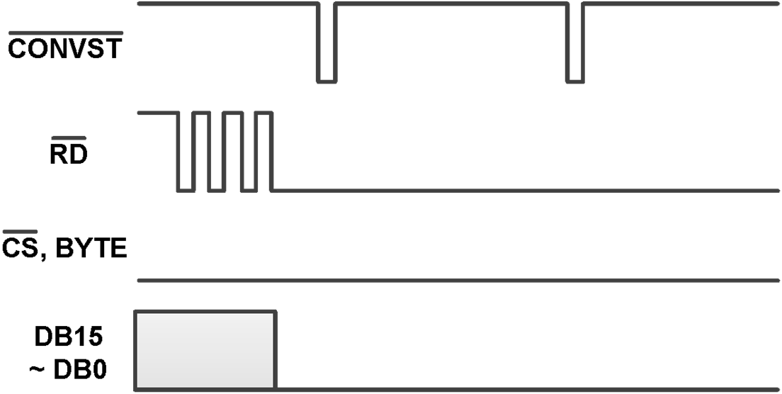
In order to minimize the number of control signals, I tied CS bar, RD bar, and BYTE to logical low, and generated only a low-toggling pulse on CONVST bar to sample the ADC input. However, I found that the ADC output remains fixed at a logical high level without changing.

According to the datasheet, RD should be toggled three times during initialization. Could the problem be caused because I did not perform this step? My understanding is that this step is only required to avoid invalid outputs from the first three conversions, and that if I only intend to use subsequent outputs, RD bar could be tied to ground. Could you please confirm whether this assumption is correct?

Thank you for your assistance.

Best regards,
Kihun Kim

  • Hi Kihun,

    Thanks for your question. Looking at the datasheet, the initialization section also mentions that the /RD toggles at power-up to load trim data to the device. This may be linked to general ADC performance as well, so I would recommend not tying /RD to logic low permanently. 

    Let me know if toggling /RD fixes your issue. If not, we can further debug!

    Best regards,

    Samiha

  • Hi Samiha,

    As you mentioned, even after toggling the /RD signal three times without tying it to ground, the ADC output still remains fixed at 1111…111 (logical high level).
    Could you please let me know what kind of waveform should be applied to the /RD signal during initialization? Additionally, I would appreciate your advice on how to properly handle the BYTE and CS pins, the other control pins.

    Since I would like to use the device in Auto Read mode, I have been applying logic low (ground) to the /CS and BYTE signals from the IC chip booting stage.

    Also, may I ask if you are selling an evaluation board for the ADS8371?

    Thank you very much.

    Best regards,
    Kihun Kim

  • Hi Kihun,

    Thanks for clarifying. Could you please share your schematic and a logic analyzer/scope screenshot of the fixed logic high output along with other digital signals? I’ll get back to you with the waveform you need to apply. 

    Best regards, 

    Samiha

  • Hi Samiha,

    During my experiment, I found some corrupted portions in the stored data, so I drew the shape of the input signal I applied as shown below. I apologize for not being able to share the experimental data itself. The logical high level is 3.3 V and the low level is 0 V.

    For the /CONVST signal, I followed the datasheet specification, setting the pulse width between 40 ns and 400 ns, and I also tried applying it with the recommended transition time from the datasheet in case transition speed was an issue. The /CS and BYTE signals were tied to 0 V (logical low) after the IC chip booting. Since there was no specific requirement stated for the /RD signal timing, I tried both narrow and wide pulse widths, but the 16 output pins still remained at 0 without any change.

    I would greatly appreciate it if you could provide detailed waveforms showing how these control pins should be applied.

    Additionally, I would like to ask whether you provide an evaluation board for the ADS8371 device.

    Thank you very much.

    Best regards,
    Kihun Kim

  • Hi Kihun,

    I understand. Unfortunately, we do not have an EVM for this device. This is an older part and my main reference material is the datasheet, so this will be difficult to debug. If you are not absolutely needing the parallel interface, I would highly recommend looking into the ADS8861 ADC instead. This is newer and the 18-bit variant has an EVM and software GUI available for your easy evaluation.

    Best regards,

    Samiha