ADS7066: Daisy Chain Communication Issue with ADS7066IYBHT Part2

Guru 12235 points
Part Number: ADS7066

Tool/software:

Hi,

In the "Related Questions" section, I will ask additional questions based on my previous interactions with the manufacturer's engineers.

We are currently supporting a customer evaluating the ADS7066IYBHT in a 5-device daisy chain configuration, and would like to confirm the following technical details regarding the SPI behavior.

1. Daisy Chain Receive Order

In the following configuration:

FPGA → ADC0 → ADC1 → ADC2 → ADC3 → ADC4 → FPGA

We understand that the input data (SDI) propagates through the chain such that each ADC receives its 24-bit command in reverse order as follows:

  • Clocks 1–24: ADC4 receives

  • Clocks 25–48: ADC3

  • Clocks 49–72: ADC2

  • Clocks 73–96: ADC1

  • Clocks 97–120: ADC0

Could you please confirm whether this interpretation matches the internal shift register behavior described in the datasheet section 7.3.10.2 Daisy-Chain Mode?

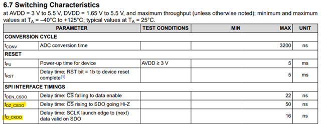
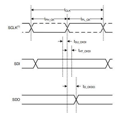
2. SPI-00 Protocol Timing Behavior

Regarding the SPI-00 protocol (default), our understanding is:

  • SDI is latched on SCLK rising edge

  • SDO updates on SCLK falling edge

Additionally, we would appreciate your clarification on:

  • Page 9 of the datasheet (Figure 6-3) appears to imply:

    • SDO becomes valid after CS falling edge + tDEN_CSDO

    • SDO toggles after SCLK rising edge + tD_CKDO

  • However, we could not find explicit timing definitions for tDEN_CSDO or tD_CKDO in the electrical characteristics table.

Do you have more detailed SPI timing charts (such as SCLK / SDI / SDO waveform diagrams), especially for Daisy Chain mode in SPI-00, that you could share?
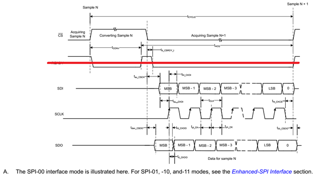
Thanks,

Conor

  • Hi Conor,

    Apologies for the delay on the response here. I will need additional time to look into this, so please expect a response by tomorrow.

    Regards,
    Joel

  • Hi Joel,

    Okay, I'll be waiting for your update.

    Thanks,

    Conor

  • Hello Connor, 

    To answer your questions:

    1. Yes, the FPGA will receive the data from the last ADC to 1st ADC order: FPGA<--ADC4<--ADC3<--ADC2<--ADC1<--ADC0
    2. I can recreate a timing diagram for the ADS7066 specifically but the one shared could work very well for SPI-00 w/enhanced SPI for the ADS7066
      1. Figure 6-1, 6-2, and 7-5 in the datasheet show this but separately 
      2.  tDEN_CSDO has a max limit of 22ns and  tD_CKDO has a max limit of 16ns (these values can be found in the 6.7 Switching Characteristics Table in the datasheet
      3. Figures 7-5 shows the SPI-00 protocol SCLK/SDO relationship as well.

    Best regards, 

    Yolanda 

  • Hi Yolanda,

    I understand the timing of when data is output to SDO as follows. Is this correct?
    • First, CS falls: SDO is enabled.
    • Next, SCLK rises: The next data is output and SDO is updated.
    • Next, SCLK falls: SDO is updated.
    In this case, is it correct to understand that SDO is updated on both the rising and falling edges of the first SCLK cycle?

    Thanks,

    Conor

  • Hi Yolanda,

    I understand the timing of when data is output to SDO as follows. Is this correct?
    • First, CS falls: SDO is enabled.
    • Next, SCLK rises: The next data is output and SDO is updated.
    • Next, SCLK falls: SDO is updated.
    In this case, is it correct to understand that SDO is updated on both the rising and falling edges of the first SCLK cycle?

    Thanks,

    Conor

  • Hello Connor, 

    So this device works with an "enhanced-SPI", it works as SPI but its timing is able to be a bit faster to enable full throughput with slower SCLKs 

    What happens with this device is:

    • First, CS Falls - SDO is enabled 
    • Next SCLK Rising Edge - SDI is latched and SDO is valid
      • there is a small delay of tD_CKDO, then SDO updates. 
    • Next SCLK Falling Edge - SDO "updates"  
      • tD_CKDO is the time from the "Launching" edge (in this case same as the SDI Latching edge) to when the SDO actually updates 
      • Because this is after the the edge that is used to read SDO, the updating edge is "rounded" to the next edge --> the falling edge.
      • This SDO is essentially updating t_CLK/2 - tD_CKDO before the falling edge (or t_PH_CLK - tD_CKDO).

    The SDO only updates once per SCLK period, because of the enhanced SPI it is earlier/quicker than typical SPI protocols. 

    Best regards, 

    Yolanda

  • Hi Yolanda,

    Thank you for your reply.

    We would like to confirm one more point regarding the SDO update timing under SPI-00 mode.

    To summarize our current understanding:
    The SDO output is updated beginning at the rising edge of SCLK, and after a delay of tD_CKDO (MAX = 16 ns), the data becomes valid.
    If the tD_CKDO minimum is 0 ns, then it would appear that the SDO is updated directly at the rising edge of SCLK.
    Based on this, we understand that the SDO is updated only once per clock cycle.
    Is it therefore correct to interpret that under SPI-00 mode, the SDO is effectively updated on the falling edge of each SCLK (as this is the time at which it is typically read)?

    We have also created a timing diagram (attached) showing our understanding of the CS/SCLK/SDI/SDO timing for SPI-00 mode during Daisy-Chain communication.
    Could you please review this diagram and let us know if there are any mistakes or misunderstandings?
    ADC SPI_daisy chain timing.xlsx

    Despite testing various timing configurations, the SDO output timing of the first ADC in the chain (ADC0) still appears incorrect, and we have not yet succeeded in establishing full Daisy-Chain operation with 5 devices.
    If Daisy-Chain communication cannot be made to work with our current setup, we may need to consider a circuit redesign.

    In this regard, we kindly ask the following questions:

    Has the ADS7066IYBHT Daisy-Chain mode been successfully verified on actual hardware in your lab or with a reference design?

    If available, could you share any example code (even in C language) that demonstrates how to operate the ADS7066 in Daisy-Chain mode?

    We appreciate your assistance and look forward to your feedback.

    Best regards,

    Conor

  • Hello Connor, 

    Thank you for the SPI timing with daisy chain. That looks good to me and I think we are aligned on the SPI-00 timing for the device. 

    I myself have tested the daisy-chain functionality using EVMs, only 3 not 5 though. This was done with a modified control set up though, so I do not have a sharable example code available. Let me attempt it again and collect some timing screen shots as well as confirm the set-up needed and share this with you. 

    In the mean time,  I know in the previous E2E thread we discussed the set-up for these devices, but just to make sure, could you share them again? 

    Is the data frame configuration default or are any status bits enabled? 

    During the daisy chain testing is has there been any register read back attempts? What about just sending NOPs?

    Could you also please share a schematic of the devices that are daisy chained? 

    Best regards, 

    Yolanda

  • Hi Yolanda,

    Thank you for your continued support. Please find our responses to your questions below:

    1. Setup details

    • Daisy chain connection: FPGA → ADC0 → ADC1 → ADC2 → ADC3 → ADC4 → FPGA

    • SCLK frequency: designed for 15 MHz

    • ADC register configuration:

      • Internal reference enabled

      • Input range set to 2 × VREF

      • CRC module disabled (default)

      • ADC offset calibrated

    To apply the above setup, after powering the board, we configure the “GENERAL_CFG” register (address: 0x01) to 0x8A.

    2. Data frame configuration
    The data frame configuration is set to default. The SPI protocol is also default (SPI-00).

    3. Register readback and NOP test
    To perform a register readback, we understand that the read command (0001 0000b), an 8-bit register address, and 8-bit dummy data must be sent. However, since daisy chain communication with the ADCs is not functioning, we have not been able to complete a readback.

    When only NOP (0x000000) is sent, the returned value from the ADCs is 0. Please see the attached image for reference.

    4. Schematic
    We will send the schematic of the ADC daisy chain connection via private message, so please approve access.

    Thanks,

    Conor

  • Hi Yolanda,

    Do you have any update?

    Thanks,

    Conor

  • Hello Connor, 

    Apologies for the delay, it has been a busy time on my end. 

    I tried the daisy chain again and it appears to work on my end with default (power-up configurations). 

    One difference with the set up I was able to set-up for this was that the system I had available is not using a continuous data stream, it sends the SPI data in packets, allowing for some time between each frame. 

    Unfortunately to be able to test the continuous clock it would take me a bit more time, could you try adding a small delay between your SPI frames?

    Best regards, 

    Yolanda 

  • Hi Yolanda,

    Just to confirm, when you suggest adding a delay between SPI frames, should this be understood as stopping the SPI clock during the delay period? For example: CS LOW → 24 clocks (Frame 0) → delay (no clock) → 24 clocks (Frame 1) … → CS HIGH.

    Best regards,
    Conor

  • Hello Connor, 

    Correct.

    Best regards, 

    Yolanda