Tool/software:
Hello,
I am working with the ADS4145 and configuring it through the SPI interface.
According to the datasheet, writing Address = 0x25, Data = 0x01 should set the ADC test pattern to zero.
However, when I perform this write, the output is not zero — I still observe varying values at the ADC output.
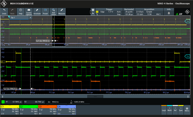
I captured the SPI signals with an oscilloscope (see attached image).
-
Yellow (C1): SEN
-
Green (C2): SCLK
-
Orange (C3): SDATA
-
Blue (C4): not connected (unused channel)
It looks like I am sending the 16-bit sequence correctly (8-bit address followed by 8-bit data, latched on falling edges). Still, the ADC does not output zeros.
Additionally, I monitored the ADC data bus using an ILA inside the FPGA (see second attached capture). The captured values continue to show non-zero random-like data rather than the expected all-zeros test pattern.
For reference, the DFS pin is hardwired to CMOS Offset Binary mode in my design.
Could you please confirm:
-
If register 0x25 = 0x01 is indeed the correct setting for forcing a zero test pattern?
-
Whether my SPI sequence (timing, SEN, number of clocks) looks correct based on the oscilloscope capture?
-
If there are any other configuration steps required before enabling the zero test pattern?
Thank you very much for your support.