Other Parts Discussed in Thread: ADC3664
Tool/software:
Hi,
I’m currently working on a prototype project where I plan to interface the ADC3564 with the ZCU106 FMC. I’ve reviewed the datasheet thoroughly and prepared a configuration script based on the register settings provided.
In this setup, the ADC will be used as a Video ADC, where a pulse-based input from a function generator will be used instead of a direct RF signal from a signal generator.
I intend to configure the chip with a basic setup, and the key requirements are as follows:
- Interface: 1-Wire (1 lane per channel)
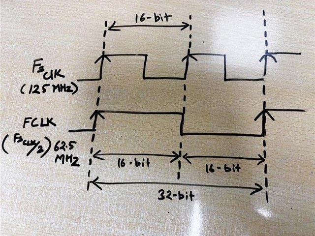
- Resolution: 16-bit
- Sampling Rate (Fs): 125 MSPS
- Decimation (DCM): x2 (Real Decimation)
- FCLK: 62.5 MHz
- DCLK/DCLKIN: 500 MHz
- NCO: Bypassed / Unused (No mixing)
- SYNC: Used for power-down (not synchronization, as only one ADC interface is used per hardware)
I’ve attached the configuration script along with a highlighted and annotated version of the datasheet. I have a few queries and would appreciate your guidance:
-
Since I’ve selected 16-bit resolution, should the zero-padding be applied to the LSB bits (D0, D1) or the MSB bits (D14, D15)?
-
Do I need to explicitly program registers 0x39 to 0x60 and 0x61 to 0x88 for the output bit mapper for Channel A and B, respectively?
- If yes, could you please verify whether the attached configuration is correct?
- I came across a note suggesting that the output bit mapping might be handled automatically based on the selected configuration. Could you confirm if manual programming is still required?
-
Is it feasible to operate the ADC with only one channel and one lane?
Lastly, could someone kindly review the attached script to verify the register configuration sequence and values? I’ve also included the updated datasheet with my highlights and comments for reference.
Thanks in advance for your support!
Best regards,
Sourav
adc3564_datasheet_with_highlights_&_comments.pdf
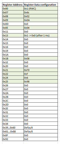
#=============================================================================
# Video ADC register configuration
# CSR BASE_ADDR : 0xA000_0000
#=============================================================================
#adc_core_reset
mrd -force 0xA0002004
mwr -force 0xA0002004 0x0
mrd -force 0xA0002004

# #################adc register configuration########################
#set this bit for soft_reset (register 0x0) (self clearing bit)
mwr -force 0xA0001008 0x0000
mwr -force 0xA000100C 0x01
mwr -force 0xA0001004 0x1
after 20
mwr -force 0xA0001008 0x8000
mwr -force 0xA0001004 0x1
mrd -force 0xA0001014

#output interface mapper (register 0x07)
#1-wire output interface mapper mode
mwr -force 0xA0001008 0x0007
mwr -force 0xA000100C 0x6c
mwr -force 0xA0001004 0x1
after 1
mwr -force 0xA0001008 0x8007
mwr -force 0xA0001004 0x1
mrd -force 0xA0001014

#e-fuse loader (register 0x13)
#wait for 1 ms,the set it to 0x0
mwr -force 0xA0001008 0x0013
mwr -force 0xA000100C 0x01
mwr -force 0xA0001004 0x1
after 1
mwr -force 0xA0001008 0x8013
mwr -force 0xA0001004 0x1
mrd -force 0xA0001014
after 1
mwr -force 0xA0001008 0x0013
mwr -force 0xA000100C 0x00
mwr -force 0xA0001004 0x1
after 1
mwr -force 0xA0001008 0x8013
mwr -force 0xA0001004 0x1
mrd -force 0xA0001014

#power down options (register 0x08)
#global power up(normal mode)
mwr -force 0xA0001008 0x0008
mwr -force 0xA000100C 0x02
mwr -force 0xA0001004 0x1
after 1
mwr -force 0xA0001008 0x8008
mwr -force 0xA0001004 0x1
mrd -force 0xA0001014

#global power down (toggle bit[0] of this register)
#mwr -force 0xA0001008 0x0008
#mwr -force 0xA000100C 0x03
#mwr -force 0xA0001004 0x1
#after 1
#mwr -force 0xA0001008 0x8008
#mwr -force 0xA0001004 0x1
#mrd -force 0xA0001014

#power down options for FLCK,DCLK,DA/DB (data lanes)(register 0x09)
#global power up(normal mode) - DA0 & DB0 powered up whereas DA1 & DB1 are powered down(1-lane per channel)
mwr -force 0xA0001008 0x0009
mwr -force 0xA000100C 0x0A
mwr -force 0xA0001004 0x1
after 1
mwr -force 0xA0001008 0x8009
mwr -force 0xA0001004 0x1
mrd -force 0xA0001014

#Global power down masking options (register 0x0D)
#For global power down (bit[0] of register 0x08 set to 1),the following interface shall get powerdown:
#(a) sampling clock input buffer
#(b) reference amplifier
#NOTE: Internal 1.2V bandgap voltage reference will NOT get powered down when global power down is exercised
mwr -force 0xA0001008 0x000D
mwr -force 0xA000100C 0x00
mwr -force 0xA0001004 0x1
after 1
mwr -force 0xA0001008 0x800D
mwr -force 0xA0001004 0x1
mrd -force 0xA0001014

#SYNC/PDN pin functionlity and REFBUF control (register 0x0E)
#sync/pdn pin shall be used for global power down mode instead of using for synchronization purpose using SPI
#The voltage reference option is selected for External voltage reference with differential sampling clock input buffer
mwr -force 0xA0001008 0x000E
mwr -force 0xA000100C 0x04
mwr -force 0xA0001004 0x1
after 1
mwr -force 0xA0001008 0x800E
mwr -force 0xA0001004 0x1
mrd -force 0xA0001014

#Differential ended analog input (register 0x11)
mwr -force 0xA0001008 0x0011
mwr -force 0xA000100C 0x00
mwr -force 0xA0001004 0x1
after 1
mwr -force 0xA0001008 0x8011
mwr -force 0xA0001004 0x1
mrd -force 0xA0001014

#Test Patterns (register 0x14/15/16)
#Normal output mode(test pattern output disabled) - default
mwr -force 0xA0001008 0x0014
mwr -force 0xA000100C 0x00
mwr -force 0xA0001004 0x1
after 1
mwr -force 0xA0001008 0x8014
mwr -force 0xA0001004 0x1
mrd -force 0xA0001014

mwr -force 0xA0001008 0x0015
mwr -force 0xA000100C 0x00
mwr -force 0xA0001004 0x1
after 1
mwr -force 0xA0001008 0x8015
mwr -force 0xA0001004 0x1
mrd -force 0xA0001014

mwr -force 0xA0001008 0x0016
mwr -force 0xA000100C 0x00
mwr -force 0xA0001004 0x1
after 1
mwr -force 0xA0001008 0x8016
mwr -force 0xA0001004 0x1
mrd -force 0xA0001014

#FCLK configuration (register 0x19)
#FCLK generated from ADC with DDC Bypass mode for 1-wire output
mwr -force 0xA0001008 0x0019
mwr -force 0xA000100C 0x00
mwr -force 0xA0001004 0x1
after 1
mwr -force 0xA0001008 0x8019
mwr -force 0xA0001004 0x1
mrd -force 0xA0001014

#LVDS swing High/low (register 0x1A)
mwr -force 0xA0001008 0x001A
mwr -force 0xA000100C 0x00
mwr -force 0xA0001004 0x1
after 1
mwr -force 0xA0001008 0x801A
mwr -force 0xA0001004 0x1
mrd -force 0xA0001014

#Output Bit mapper disabled(due to Real Decimation mode being used) & 16-bit resolution set (register 0x1B)
mwr -force 0xA0001008 0x001B
mwr -force 0xA000100C 0x08
mwr -force 0xA0001004 0x1
after 1
mwr -force 0xA0001008 0x801B
mwr -force 0xA0001004 0x1
mrd -force 0xA0001014

#SLVDS output data & DCLK delay (register 0x1E) - default
mwr -force 0xA0001008 0x001E
mwr -force 0xA000100C 0x00
mwr -force 0xA0001004 0x1
after 1
mwr -force 0xA0001008 0x801E
mwr -force 0xA0001004 0x1
mrd -force 0xA0001014

#FCLK pattern for 1-wire 16 bit resolution (register 0x20/21/22)
mwr -force 0xA0001008 0x0020
mwr -force 0xA000100C 0x00
mwr -force 0xA0001004 0x1
after 1
mwr -force 0xA0001008 0x8020
mwr -force 0xA0001004 0x1
mrd -force 0xA0001014

mwr -force 0xA0001008 0x0021
mwr -force 0xA000100C 0xF0
mwr -force 0xA0001004 0x1
after 1
mwr -force 0xA0001008 0x8021
mwr -force 0xA0001004 0x1
mrd -force 0xA0001014

mwr -force 0xA0001008 0x0022
mwr -force 0xA000100C 0x0F
mwr -force 0xA0001004 0x1
after 1
mwr -force 0xA0001008 0x8022
mwr -force 0xA0001004 0x1
mrd -force 0xA0001014

#DDC enabled and datapath shall include digital features (register 0x24)
mwr -force 0xA0001008 0x0024
mwr -force 0xA000100C 0x06
mwr -force 0xA0001004 0x1
after 1
mwr -force 0xA0001008 0x8024
mwr -force 0xA0001004 0x1
mrd -force 0xA0001014

#DDC Mux enabled, DCM : x2 ,Real decimation, NCO phase as it is (register 0x25)
mwr -force 0xA0001008 0x0025
mwr -force 0xA000100C 0x98
mwr -force 0xA0001004 0x1
after 1
mwr -force 0xA0001008 0x8025
mwr -force 0xA0001004 0x1
mrd -force 0xA0001014

#No Digital Gain added for accounting NCO mixing loss for ADC channel A & B since Real
#decimation is selected and Fs/4 mixing is disabled for both the channels(register 0x26) -default
mwr -force 0xA0001008 0x0026
mwr -force 0xA000100C 0x00
mwr -force 0xA0001004 0x1
after 1
mwr -force 0xA0001008 0x8026
mwr -force 0xA0001004 0x1
mrd -force 0xA0001014

#Output order of I & Q data is not inverted/swapped of channel A (register 0x27) -default
mwr -force 0xA0001008 0x0027
mwr -force 0xA000100C 0x00
mwr -force 0xA0001004 0x1
after 1
mwr -force 0xA0001008 0x8027
mwr -force 0xA0001004 0x1
mrd -force 0xA0001014

#NCO configuration FTW registers (unused) of channel A (register 0x2A/2B/2C/2D) -default
mwr -force 0xA0001008 0x002A
mwr -force 0xA000100C 0x00
mwr -force 0xA0001004 0x1
after 1
mwr -force 0xA0001008 0x802A
mwr -force 0xA0001004 0x1
mrd -force 0xA0001014

mwr -force 0xA0001008 0x002B
mwr -force 0xA000100C 0x00
mwr -force 0xA0001004 0x1
after 1
mwr -force 0xA0001008 0x802B
mwr -force 0xA0001004 0x1
mrd -force 0xA0001014

mwr -force 0xA0001008 0x002C
mwr -force 0xA000100C 0x00
mwr -force 0xA0001004 0x1
after 1
mwr -force 0xA0001008 0x802C
mwr -force 0xA0001004 0x1
mrd -force 0xA0001014

mwr -force 0xA0001008 0x002D
mwr -force 0xA000100C 0x00
mwr -force 0xA0001004 0x1
after 1
mwr -force 0xA0001008 0x802D
mwr -force 0xA0001004 0x1
mrd -force 0xA0001014

#Output order of I & Q data is not inverted/swapped of channel B (register 0x2E) -default
mwr -force 0xA0001008 0x002E
mwr -force 0xA000100C 0x00
mwr -force 0xA0001004 0x1
after 1
mwr -force 0xA0001008 0x802E
mwr -force 0xA0001004 0x1
mrd -force 0xA0001014

#NCO configuration FTW registers (unused) of channel B (register 0x31/32/33/34) -default
mwr -force 0xA0001008 0x0031
mwr -force 0xA000100C 0x00
mwr -force 0xA0001004 0x1
after 1
mwr -force 0xA0001008 0x8031
mwr -force 0xA0001004 0x1
mrd -force 0xA0001014

mwr -force 0xA0001008 0x0032
mwr -force 0xA000100C 0x00
mwr -force 0xA0001004 0x1
after 1
mwr -force 0xA0001008 0x8032
mwr -force 0xA0001004 0x1
mrd -force 0xA0001014

mwr -force 0xA0001008 0x0033
mwr -force 0xA000100C 0x00
mwr -force 0xA0001004 0x1
after 1
mwr -force 0xA0001008 0x8033
mwr -force 0xA0001004 0x1
mrd -force 0xA0001014

mwr -force 0xA0001008 0x0034
mwr -force 0xA000100C 0x00
mwr -force 0xA0001004 0x1
after 1
mwr -force 0xA0001008 0x8034
mwr -force 0xA0001004 0x1
mrd -force 0xA0001014

#Output Bit mapper for channel DA0 (1-wire 16 bit resolution mode) -optional (register 0x39 to 0x60)
#mwr -force 0xA0001008 0x004C
#mwr -force 0xA000100C 0x46
#mwr -force 0xA0001004 0x1
#after 1
#mwr -force 0xA0001008 0x804C
#mwr -force 0xA0001004 0x1
#mrd -force 0xA0001014
#
#mwr -force 0xA0001008 0x004B
#mwr -force 0xA000100C 0x47
#mwr -force 0xA0001004 0x1
#after 1
#mwr -force 0xA0001008 0x804B
#mwr -force 0xA0001004 0x1
#mrd -force 0xA0001014
#
#mwr -force 0xA0001008 0x004A
#mwr -force 0xA000100C 0x4C
#mwr -force 0xA0001004 0x1
#after 1
#mwr -force 0xA0001008 0x804A
#mwr -force 0xA0001004 0x1
#mrd -force 0xA0001014
#
#mwr -force 0xA0001008 0x0049
#mwr -force 0xA000100C 0x4D
#mwr -force 0xA0001004 0x1
#after 1
#mwr -force 0xA0001008 0x8049
#mwr -force 0xA0001004 0x1
#mrd -force 0xA0001014
#
#mwr -force 0xA0001008 0x0048
#mwr -force 0xA000100C 0x4E
#mwr -force 0xA0001004 0x1
#after 1
#mwr -force 0xA0001008 0x8048
#mwr -force 0xA0001004 0x1
#mrd -force 0xA0001014
#
#mwr -force 0xA0001008 0x0047
#mwr -force 0xA000100C 0x4F
#mwr -force 0xA0001004 0x1
#after 1
#mwr -force 0xA0001008 0x8047
#mwr -force 0xA0001004 0x1
#mrd -force 0xA0001014
#
#mwr -force 0xA0001008 0x0046
#mwr -force 0xA000100C 0x54
#mwr -force 0xA0001004 0x1
#after 1
#mwr -force 0xA0001008 0x8046
#mwr -force 0xA0001004 0x1
#mrd -force 0xA0001014
#
#mwr -force 0xA0001008 0x0045
#mwr -force 0xA000100C 0x55
#mwr -force 0xA0001004 0x1
#after 1
#mwr -force 0xA0001008 0x8045
#mwr -force 0xA0001004 0x1
#mrd -force 0xA0001014
#
#mwr -force 0xA0001008 0x0044
#mwr -force 0xA000100C 0x56
#mwr -force 0xA0001004 0x1
#after 1
#mwr -force 0xA0001008 0x8044
#mwr -force 0xA0001004 0x1
#mrd -force 0xA0001014
#
#mwr -force 0xA0001008 0x0043
#mwr -force 0xA000100C 0x57
#mwr -force 0xA0001004 0x1
#after 1
#mwr -force 0xA0001008 0x8043
#mwr -force 0xA0001004 0x1
#mrd -force 0xA0001014
#
#mwr -force 0xA0001008 0x0042
#mwr -force 0xA000100C 0x5C
#mwr -force 0xA0001004 0x1
#after 1
#mwr -force 0xA0001008 0x8042
#mwr -force 0xA0001004 0x1
#mrd -force 0xA0001014
#
#mwr -force 0xA0001008 0x0041
#mwr -force 0xA000100C 0x5D
#mwr -force 0xA0001004 0x1
#after 1
#mwr -force 0xA0001008 0x8041
#mwr -force 0xA0001004 0x1
#mrd -force 0xA0001014
#
#mwr -force 0xA0001008 0x0040
#mwr -force 0xA000100C 0x5E
#mwr -force 0xA0001004 0x1
#after 1
#mwr -force 0xA0001008 0x8040
#mwr -force 0xA0001004 0x1
#mrd -force 0xA0001014
#
#mwr -force 0xA0001008 0x003F
#mwr -force 0xA000100C 0x5F
#mwr -force 0xA0001004 0x1
#after 1
#mwr -force 0xA0001008 0x803F
#mwr -force 0xA0001004 0x1
#mrd -force 0xA0001014
#
#mwr -force 0xA0001008 0x003E
#mwr -force 0xA000100C 0x64
#mwr -force 0xA0001004 0x1
#after 1
#mwr -force 0xA0001008 0x803E
#mwr -force 0xA0001004 0x1
#mrd -force 0xA0001014
#
#mwr -force 0xA0001008 0x003D
#mwr -force 0xA000100C 0x65
#mwr -force 0xA0001004 0x1
#after 1
#mwr -force 0xA0001008 0x803D
#mwr -force 0xA0001004 0x1
#mrd -force 0xA0001014

#Output Bit mapper for channel DB0 (1-wire 16 bit resolution mode) -optional (register 0x61 to 0x88)
#mwr -force 0xA0001008 0x0074
#mwr -force 0xA000100C 0x42
#mwr -force 0xA0001004 0x1
#after 1
#mwr -force 0xA0001008 0x8074
#mwr -force 0xA0001004 0x1
#mrd -force 0xA0001014
#
#mwr -force 0xA0001008 0x0073
#mwr -force 0xA000100C 0x43
#mwr -force 0xA0001004 0x1
#after 1
#mwr -force 0xA0001008 0x8073
#mwr -force 0xA0001004 0x1
#mrd -force 0xA0001014
#
#mwr -force 0xA0001008 0x0072
#mwr -force 0xA000100C 0x48
#mwr -force 0xA0001004 0x1
#after 1
#mwr -force 0xA0001008 0x8072
#mwr -force 0xA0001004 0x1
#mrd -force 0xA0001014
#
#mwr -force 0xA0001008 0x0071
#mwr -force 0xA000100C 0x49
#mwr -force 0xA0001004 0x1
#after 1
#mwr -force 0xA0001008 0x8071
#mwr -force 0xA0001004 0x1
#mrd -force 0xA0001014
#
#mwr -force 0xA0001008 0x0070
#mwr -force 0xA000100C 0x4A
#mwr -force 0xA0001004 0x1
#after 1
#mwr -force 0xA0001008 0x8070
#mwr -force 0xA0001004 0x1
#mrd -force 0xA0001014
#
#mwr -force 0xA0001008 0x006F
#mwr -force 0xA000100C 0x4B
#mwr -force 0xA0001004 0x1
#after 1
#mwr -force 0xA0001008 0x806F
#mwr -force 0xA0001004 0x1
#mrd -force 0xA0001014
#
#mwr -force 0xA0001008 0x006E
#mwr -force 0xA000100C 0x50
#mwr -force 0xA0001004 0x1
#after 1
#mwr -force 0xA0001008 0x806E
#mwr -force 0xA0001004 0x1
#mrd -force 0xA0001014
#
#mwr -force 0xA0001008 0x006D
#mwr -force 0xA000100C 0x51
#mwr -force 0xA0001004 0x1
#after 1
#mwr -force 0xA0001008 0x806D
#mwr -force 0xA0001004 0x1
#mrd -force 0xA0001014
#
#mwr -force 0xA0001008 0x006C
#mwr -force 0xA000100C 0x52
#mwr -force 0xA0001004 0x1
#after 1
#mwr -force 0xA0001008 0x806C
#mwr -force 0xA0001004 0x1
#mrd -force 0xA0001014
#
#mwr -force 0xA0001008 0x006B
#mwr -force 0xA000100C 0x53
#mwr -force 0xA0001004 0x1
#after 1
#mwr -force 0xA0001008 0x806B
#mwr -force 0xA0001004 0x1
#mrd -force 0xA0001014
#
#mwr -force 0xA0001008 0x006A
#mwr -force 0xA000100C 0x58
#mwr -force 0xA0001004 0x1
#after 1
#mwr -force 0xA0001008 0x806A
#mwr -force 0xA0001004 0x1
#mrd -force 0xA0001014
#
#mwr -force 0xA0001008 0x0069
#mwr -force 0xA000100C 0x59
#mwr -force 0xA0001004 0x1
#after 1
#mwr -force 0xA0001008 0x8069
#mwr -force 0xA0001004 0x1
#mrd -force 0xA0001014
#
#mwr -force 0xA0001008 0x0068
#mwr -force 0xA000100C 0x5A
#mwr -force 0xA0001004 0x1
#after 1
#mwr -force 0xA0001008 0x8068
#mwr -force 0xA0001004 0x1
#mrd -force 0xA0001014
#
#mwr -force 0xA0001008 0x0067
#mwr -force 0xA000100C 0x5B
#mwr -force 0xA0001004 0x1
#after 1
#mwr -force 0xA0001008 0x8067
#mwr -force 0xA0001004 0x1
#mrd -force 0xA0001014
#
#mwr -force 0xA0001008 0x0066
#mwr -force 0xA000100C 0x60
#mwr -force 0xA0001004 0x1
#after 1
#mwr -force 0xA0001008 0x8066
#mwr -force 0xA0001004 0x1
#mrd -force 0xA0001014
#
#mwr -force 0xA0001008 0x0065
#mwr -force 0xA000100C 0x61
#mwr -force 0xA0001004 0x1
#after 1
#mwr -force 0xA0001008 0x8065
#mwr -force 0xA0001004 0x1
#mrd -force 0xA0001014

#2's complement output data format of channel A (register 0x8F) -default
mwr -force 0xA0001008 0x008F
mwr -force 0xA000100C 0x00
mwr -force 0xA0001004 0x1
after 1
mwr -force 0xA0001008 0x808F
mwr -force 0xA0001004 0x1
mrd -force 0xA0001014

#2's complement output data format of channel B (register 0x92) -default
mwr -force 0xA0001008 0x0092
mwr -force 0xA000100C 0x00
mwr -force 0xA0001004 0x1
after 1
mwr -force 0xA0001008 0x8092
mwr -force 0xA0001004 0x1
mrd -force 0xA0001014