ADS124S08: Requesting data conversion SW implement guide#2

Part Number: ADS124S08

Tool/software:

As I mentioned earlier, I implemented the software to read analog values using the ASD124S08. While testing the communication, I came across some questions that I’d like to ask.

First, I used the Continuous Conversion Mode for data conversion. At initialization, I set the registers as shown below, then periodically updated the INPMUX and IDACMUX values, switching channels and reading different analog inputs using the RDATA command.

ID: 0x00 (ADS124S08)
STATUS: 0x80
INPMUX: Channel1 (AIN1, AIN2), Channel2 (AIN5, AIN6), Channel3 (AIN9, AIN10)
PGA: 0xEA
DATARATE: 0x14
REF: 0x01
IDACMAG: 0x07
IDACMUX: Channel1 (AIN3, AIN0), Channel2 (AIN7, AIN4), Channel3 (AIN11, AIN8)
VBIAS: 0x00
SYS: 0x10

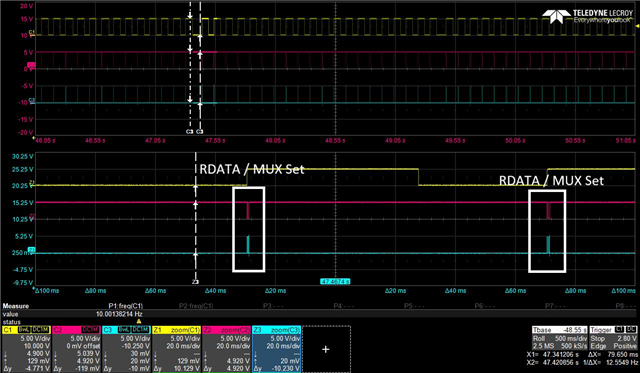
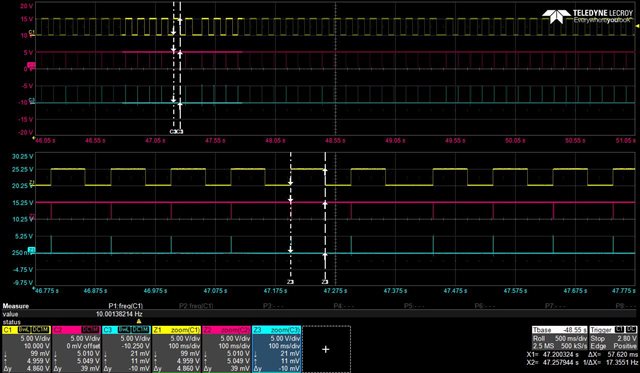
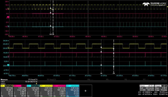
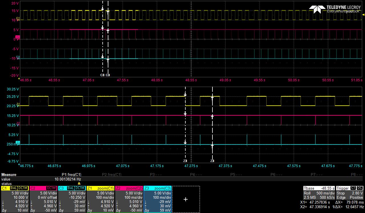
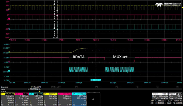
In this way, I confirmed the waveforms shown in the attached image: yellow = DRDY, red = CS, blue = SCLK.

Here are my questions:

  1. I set SPS = 20, so I expected the DRDY (HIGH period) to correspond to a conversion time of about 50 ms. In fact, I measured it at 53–57 ms. Is this 3–7 ms deviation caused by conversion delay?
    Currently, the PGA setting is configured as 1 × tMOD. Could this setting be affecting the timing?

  2. I also want to clarify the exact condition for when DRDY goes LOW. While the LOW duration is usually consistent, I sometimes observe it being maintained longer. Since I am using continuous conversion, I thought the DRDY timing would be determined strictly by the SPS setting, but it doesn’t seem consistent. I tested changing the PGA delay setting, but it didn’t affect this behavior. Could you please explain why this happens?

                   
  3. As I mentioned, I periodically update the INPMUX and IDACMUX registers using the WREG command, then read the data using RDATA. However, unless I add a delay of about 100 ms after changing the MUX settings, no valid data is read. If I reduce the delay to 50 ms, I still get invalid results. I understand that some delay should be needed after switching the MUX, but requiring such a long delay seems unusual, so I suspect I may be doing something incorrectly.

  4. In the image, the longer blue waveform on the right shows the part where I set INPMUX and IDACMUX one by one using WREG, while the left side shows the RDATA portion of the previous cycle


    In fact, after setting INPMUX and IDACMUX with WREG, I then wait until the next DRDY goes LOW and then HIGH again, and at that point I read the data using RDATA. 
    Could you please advise if you know what state this behavior corresponds to, or what I might be missing?
  • Hi Joowhan Chae,

    Some feedback regarding your questions

    I set SPS = 20, so I expected the DRDY (HIGH period) to correspond to a conversion time of about 50 ms. In fact, I measured it at 53–57 ms. Is this 3–7 ms deviation caused by conversion delay?
    Currently, the PGA setting is configured as 1 × tMOD. Could this setting be affecting the timing?
    I also want to clarify the exact condition for when DRDY goes LOW. While the LOW duration is usually consistent, I sometimes observe it being maintained longer. Since I am using continuous conversion, I thought the DRDY timing would be determined strictly by the SPS setting, but it doesn’t seem consistent. I tested changing the PGA delay setting, but it didn’t affect this behavior. Could you please explain why this happens?

    Note that the ADC conversion latency time starts after you read out the data and after you change the mux. You should be looking at this on your scope instead of just the time between DRDY. In other words, measure between the end of the last command (I assume this is WREG to INPMUX) and the transition on DRDY from high to low. If your controller is performing other tasks while the mux switching and data reading is ongoing then the time between conversions or length of DRDY might be non deterministic

    As I mentioned, I periodically update the INPMUX and IDACMUX registers using the WREG command, then read the data using RDATA. However, unless I add a delay of about 100 ms after changing the MUX settings, no valid data is read. If I reduce the delay to 50 ms, I still get invalid results. I understand that some delay should be needed after switching the MUX, but requiring such a long delay seems unusual, so I suspect I may be doing something incorrectly.

    Can you clarify what you mean by "no valid data"? How inaccurate is the data compared to the data you expect? If you measure the data continuously immediately after switching the INPMUX + IDACMUX registers, do you see the data increasing / decreasing i.e. settling to a final value? If so, this indicates a settling issue that is likely due to the capacitance on the IDAC pin. Please post your measurement data - ADC codes in hex only - so we can review

    n fact, after setting INPMUX and IDACMUX with WREG, I then wait until the next DRDY goes LOW and then HIGH again, and at that point I read the data using RDATA. Could you please advise if you know what state this behavior corresponds to, or what I might be missing?

    Your firmware should do the following:

    • Perform initialization
    • Start conversions
    • Wait for DRDY to drop low
    • Clock out data
    • Change INPMUX settings (and/or IDACMUX)
    • Wait for DRDY to drop low
    • Clock out data
    • Change INPMUX settings (and/or IDACMUX)
    • etc.

    So, you do not need to wait for DRDY to return high before clocking out data. Instead, send the RDATA command and start clocking out data as soon as DRDY transitions from high to low.

    -Bryan

  • By "no valid data" I mean the 3 bytes returned by the RDATA command contain only zero

  • Hi Joowhan Chae,

    You will get all zeros from the ADC if you try to read data before DRDY drops low and after you switch channels. If you are always reading data after DRDY transitions high to low you should not see this issue

    -Bryan