Tool/software:
Hi,
I am working with the ADC3563 and trying to verify all LVDS lanes using the built-in ramp test pattern. My setup is configured for dual-band complex decimation by 32, so I expect to see the same ramp pattern on both the DA and DB lanes. I prepared this question with the help of AI, but it really showcases my problem. The AI just finds better explanations ;-). I hope you don't mind.
Observation:
-
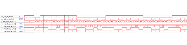
The DA lanes (DA0/DA1) are working correctly. I see a synchronous data pattern that matches the FCLK and DCLK. I have not yet deserialized the data inside the FPGA.
-
The DB lanes (DB0/DB1) are not working. I see a high-frequency, asynchronous signal that looks like noise.
System Configuration:
-
Device: ADC3563
-
Sample Clock (Fs): 15.3104 MHz
-
Serializer Clock (DCLKIN): 3.8276 MHz
-
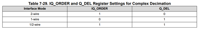
Mode: 2-Wire, 16-bit, Complex Decimation by 32, Dual-Band
-
Hardware: External 100-ohm differential termination is verified to be present on all LVDS input pairs (DA and DB) at the FPGA.
Register Initialization Sequence
Here is the exact sequence of SPI writes I am sending to the device after a hardware reset:
My Question:
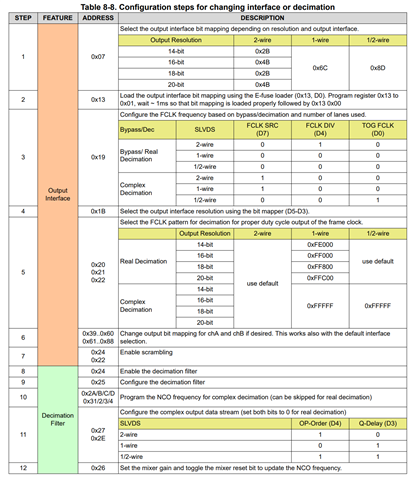
Given that the DA lanes are working plausible with this configuration, is there any register setting I have missed that is required to fully enable the DDC B data path and the DB0/DB1 LVDS drivers? The configuration seems correct according to the datasheet, but the behavior on the DB lanes indicates a problem.
Thank you for your support.