Tool/software:
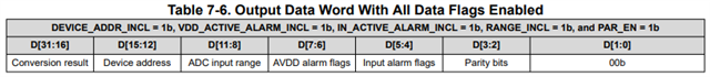
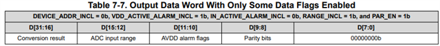
Hello - I have a custom board with an ADS8681 controlled by a FPGA. My SPI interface is working, I can set the data output reg to output 01 or 0011 and the 16 bit data returned is either x5555 or x3333. If I ground the input to the ADC I get x8000 (+/- 3 LSb) for the ADC data. I configure the rst_pwrctl_reg to enable both the input alarm and AVDD alarm, than set in the data output reg, I set bits 13:10 to '1111' so I can get both the high and low flags for both alarms. My question is where will the hi and lo alarm bits be set if an alarm is triggered? On pg 42, table 7-6 and 7-7 have the alarm flags in different bit locations. I don't need the device address or input range or parity bits, just the adc data and 4 bit alarm flags. These flags will be used to shutdown another part of the system. Thank you.