Other Parts Discussed in Thread: LMX2592, , TPS7A94, TPS7A15, TPS7N53
Tool/software:
Planning to use DDS39RFS10 in DDS only mode w/ DES (both DES2XL and DES2XH). Clocked with LMX2592 at ~7.1 GHz Fclk. Need some clarification on these points.
- Fclk leakage amplitude (in -dBFS terms) at DAC output (after balun), across 7-10 GHz Fclk range.
- Image spur amplitude when fundamental is right next to it, in DES mode. Ex: 4.9 GHz tone and its 5.1 GHz image spur (assuming 10 GHz Fclk).
- TI's recommended solution for seamlessly covering 3-7 GHz (with a single DAC), or across nyquist windows regardless of Fclk. Change the input clock, external mixing, etc.
- In DDS mode: Does a CLK frequency change need some sync time or is it instant and we only need to update the NCO frequency based on the new Fclk? Not talking about external PLL lock times, assume instant change.
- Is <1 µVrms noise LDO (TPS7A94) essential or would anything below 10µV be good enough for VDDCLK10 and other sensitive rails? LDOs like TPS7A15 / TPS7A14 would allow for 1.2V -> 1.0V
- Can VDDT (SerDes termination supply) be left unconnected or just simplified with very few decoup caps, when operating in DDS only mode?
- Can all the SerDes lanes be left unconnected (rather than GND), including all 16 JESD pairs (part of the full DAC39RF chip)? The DDS39 datasheet lists them all as DGND (other than 6 and 14) but DAC39 datasheet lists all the pins. This post mentions they can be left floating.
- Would the TCM2-722X+ balun work fine for the outputs? The eval board sch used a 3 dB T-attenuator (but 50 Ohm impedance?), is this necessary when the balun is well-matched? Or is the DAC output itself not a perfect 100ohm diff? S-parameters would help here.
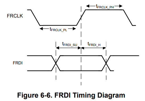
- Does FR (Fast Reconfiguration Interface) have some undocumented DDR mode for FRCLK? (Figure 6-6. FRDI Timing Diagram) looks a bit misleading in that regard. Would prefer DDR, if possible.