A related question is a question created from another question. When the related question is created, it will be automatically linked to the original question.
If you have a related question, please click the "Ask a related question" button in the top right corner. The newly created question will be automatically linked to this question.
Would you also be able to show the current HW configuration of both the TSWDC155EVM and the ADS9327EVM? A picture would help, but at least a description of the jumpers/shunts populated on both boards
Could you also scroll down to the bottom of the error window to see the full error message? or if you could copy and paste the full text that would also be helpful.
An updated version of the GUI has been released to fix the issue share, could you please install the latest version of the GUI and see if the issue is still there?
SPIM_AFE_Write(0x02); // add SPIM_AFE_Write(0x00); // SPIM_AFE_Write(0x02); // sel reg bank 1 CyDelayUs(microsecDelay);
SPIM_AFE_Write(0x0C); // add SPIM_AFE_Write(0x12); // internal ref is active SPIM_AFE_Write(0x00); // internal ref is active CyDelay(25); // requier by datasheey
SPIM_AFE_Write(0x0C); // add SPIM_AFE_Write(0x02); // internal ref is active SPIM_AFE_Write(0x00); // internal ref is active CyDelayUs(microsecDelay);
SPIM_AFE_Write(0x03); // add SPIM_AFE_Write(0x00); // unlock reg bank2 SPIM_AFE_Write(0x0B); // sel reg bank 2 CyDelayUs(microsecDelay);
SPIM_AFE_Write(0x00); // to make it 48 clk fram SPIM_AFE_Write(0x00); // to make it 48 clk fram SPIM_AFE_Write(0x00); // to make it 48 clk fram
CyDelayUs(microsecDelay);
SPIM_AFE_Write(0x02); // add SPIM_AFE_Write(0x00); // SPIM_AFE_Write(0x02); // sel reg bank 1
SPIM_AFE_Write(0x00); // to make it 48 clk fram SPIM_AFE_Write(0x00); // to make it 48 clk fram SPIM_AFE_Write(0x00); // to make it 48 clk fram
CyDelayUs(microsecDelay);
SPIM_AFE_Write(0x01); //add SPIM_AFE_Write(0x00); // SPIM_AFE_Write(0x01); // data on D3 only
SPIM_AFE_Write(0x00); // to make it 48 clk fram SPIM_AFE_Write(0x00); // to make it 48 clk fram SPIM_AFE_Write(0x00); // to make it 48 clk fram
CyDelayUs(microsecDelay); //------------------------------------------------------- Cy_GPIO_Write(P9_2_PORT, P9_2_NUM, 0x01); // stat thaking ADC sample CyDelayUs(2); Cy_GPIO_Write(P9_2_PORT, P9_2_NUM, 0x00); // stat thaking ADC sample CyDelayUs(1);
SPIM_AFE_Write(0x01); //add SPIM_AFE_Write(0x00); // SPIM_AFE_Write(0x00); // data on D3 only SPIM_AFE_Write(0x00); SPIM_AFE_Write(0x00); SPIM_AFE_Write(0x00); // CyDelayUs(microsecDelay);
Every time you need to write to the registers, the register needs to be unlocked
You need to perform the "UNLOCK Frame1" and "UNLOCK Frame2" then the Reset command. As follows:
Unlock Frame 1
Unlock Frame 2
Reset
Delay ~1ms
When enabling 1-Lane mode (setting NUM_DATA_LINES = 110b) the next frame is required to be be 48 clocks long
Not providing the full 48 clocks after it has been enabled could set the device in an unknown state.
This also means that as long as 1-Lane is enabled (until NUM_DATA_LINES ≠ 110b) the data frame should be 48 clocks, or until the device is power cycled or reset
If writing to the device to reset with 1-Lane still enabled, the data frame should be 48 clocks.
When reading back conversion data from the ADC in 1-lane mode 48 clocks are also required
The data out format will be {ADCA[15:0],0x00,ADCB[15:0],0x00}
You are correct, the Table 7-7 does not include the initial register unlock that is needed, this will be changed in the next datasheet update soon.
You only need to do the reset during the initialization process. If you reset the device every time you write to the registers this will undo all the configurations done during initialization.
Because the data format is {ADCA[15:0],0x00,ADCB[15:0],0x00} I suspect your logic analyzer might be reading the data wrong or there is a timing issue that needs to be adjusted with the communication.
Would 0x603E make more sense for ADC A? it does appear that ADC B has a full scale read, is the input on that channel more than 4.096V (or more than 8.192V differential?) Could you also confirm the common more value of both channels?
Could you share a more zoomed in screen shot of the data analysis or would you have a way to collect this with an oscilloscope?
DC input is ok, is it still going through the THS on the EVM? Please make sure that the input common mode meets the requirements
At start-up the device is configured with 4-lane mode, so all D[3:0] will be output ADC convert data. The initial data should be ignored right after power up though.
Most registers are set to 0h by default so to confirm functionality I would recommend configuring a register and reading back on D3.
If you currently cannot read any register back then there is a timing issue in the data communication. Could you please share more information on how the timing is configured? What is the SCLK frequency? What about the SAMPL_CLK frequency?
Thank you for sharing the SPI timing, the SPI_2_ADS9327 looks good. I haven't looked through the full excel file yet, but could you please share the common mode measurements as well as what the inputs look at the AIN pins?
The ADS9327 is a differential input SAR ADC, and it requires that the AINP-AINM have a common mode input of VCMOUT ± 0.4V. VCMOUT should be 2.24V ± 0.04V.
If using the ADS9327EVM you can short one of the AINM signal paths before the THS4552 via J14, J16, or J8 or J10 and input your signal on AINP via J9 or J7. This would work because the common mode will be taken care of by the THS4552.
If the THS4552 is skipped and inputs are directly input to the AINP/AINM of the ADS9327 then extra care is needed to ensure that the input common mode requirements are met as well as that the source used can the drive the inputs of the ADS9327.
From the picture you shared it appears that the THS4552 is being skipped and input common mode is not being accounted for.
Could you please try this test with those inputs before the THS4552?
Additionally I will like to add that this device does have a planned single-ended version to be released soon. The current version though is not capable of single ended functionality.
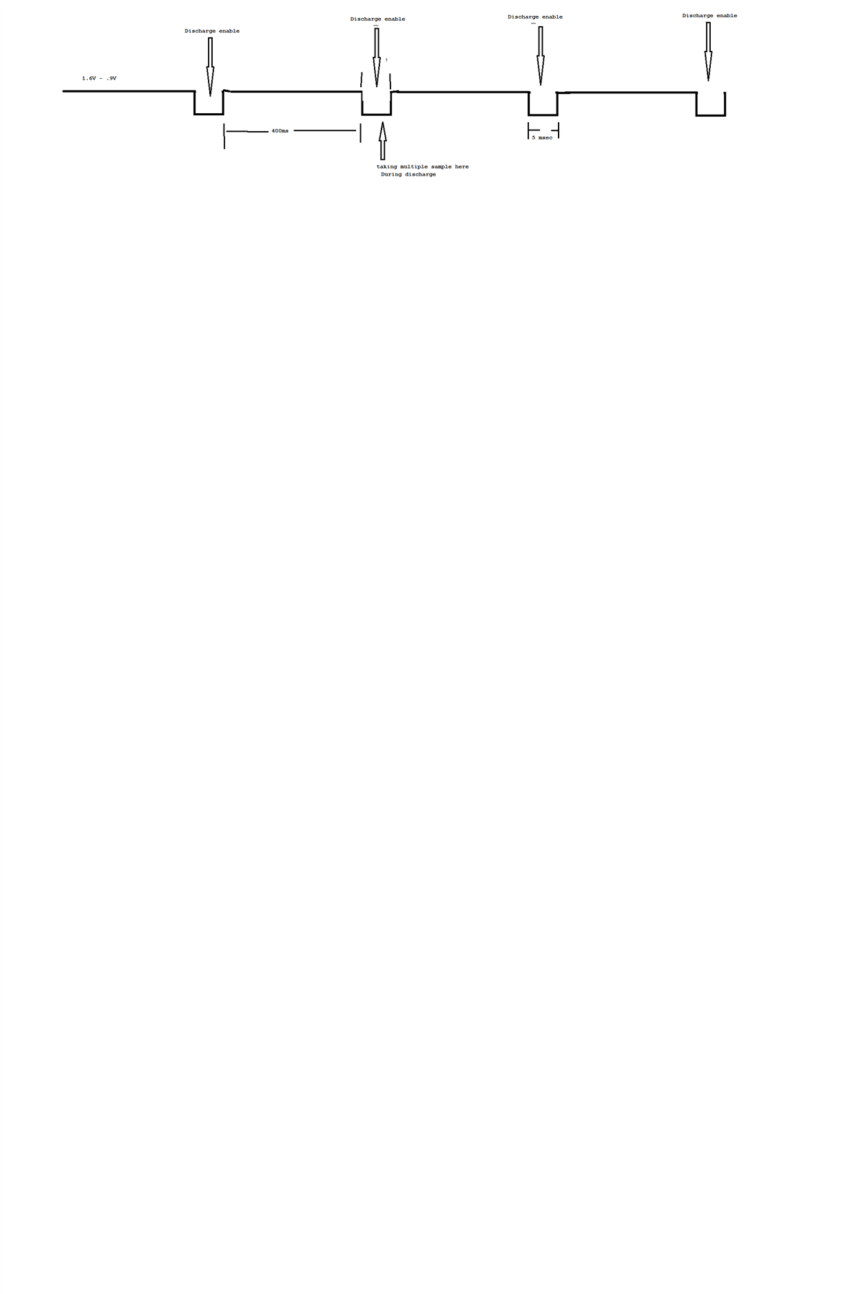
Other replacements that could measure the 5ms voltage drop, probably. What would be the the sample rate or sample count you would need for the attached signal?
Could anything else be added between your current board and the signal to add a common mode offset?
That still leaves a lot of possibilities, could you help me narrow it down a bit?
It seems like you would need a 2-ch Single-Ended ADC with SPI? with at least 12bits ? or would 16+bits be preferred?
When you mention "5msec" multiple sampling, do you mean a single sample every 5 milli-seconds or do you mean 5 million samples per second (5MSPS)?
Also, "multiple sampling" meaning simultaneous sampling? do all 32 channels need to be sampled at the same time or just 2 at a time?
If the measurement frequency is slow, there isn't much concern, but if there is a need to make measurements at around 5MSPS, an ADC Driver plus a kick-back charge RC would be required, or very heavily recommended. For fully differential ADCs a common mode consideration would also be required.
Or looking for an ADC that has integrated driver stage would be best.
We do have some options:
ADS9813: 18-bit, 8-channel, simultaneous sampling, 2MSPS, with integrated PGA (easier to drive without additional common mode driver stage like in your case).
ADS9212: 18-bit, 2-channel, simultaneous sampling, 8MSPS, with integrated PGA similar to the ADS9813
ADS8686S: 16-bit, 16-channel, simultaneous sampling with 2 channels at a time with internal mux to allow the 16 channels, 1MSPS, with integrated PGA similar to the ADS9813.
ADS8355/ADS7853/ADS7253: 16/14/12 bit (respectively), 2-channel, simultaneous sampling, 1MSPS. These could work without a driver but a slower speeds. the low side input pin can be shorted to ground though.