DAC60508: DAC60508ZC: Unable to get any value at the OUTPUT Pin

Part Number: DAC60508
Other Parts Discussed in Thread: AM6442,

Tool/software:

Hello,

We are using the DAC60508ZC device which is connected to MPU AM6442 SPI bus. With respect to SPI lines when we start the communication on SPI bus we could see CS going LOW and also the SCK and MOSI getting toggled accordingly. Since this chip doesn't support SDO functionality we can not confirm if the write is success or not and we can also not read the device ID.

we have made sure that we are writing the CLR-MSK bit for Channel 0 to 3 and Channel 4 to 7 in the GAIN register and also made sure that the internal reference voltage of 2.5V is been generated in the REF pin of the chip.

below is the sequence of register we are writing 

1. write CONFIG register with value 0x0

2. write GAIN register with 0xFF

3. write the data to DAC channels

4.  setting 4th pin of trigger register to 1

with all these reg setting also we are not able to see any Vout getting generated and it always seems to be 0V. also attached the code snippet for your reference.

Can you confirm if the sequence of the writing the register is correct or any changes is needed in the sequence.

It would be helpful if you provide us with any sample baremetal or c code for this chip.

Below is the code snippet of our application:

#include <stdio.h>

#include <stdint.h>

#include <fcntl.h>

#include <unistd.h>

#include <sys/ioctl.h>

#include <linux/spi/spidev.h>

#define SPI_DEV "/dev/spidev2.0"

#define SPI_MODE SPI_MODE_0

#define SPI_SPEED 1000000 // 1 MHz

#define SPI_BITS 8

// DAC60508 Register Addresses

#define REG_NOP 0x00

#define REG_DEVICE_CONFIG 0x01

#define REG_SHDN 0x02


#define REG_CONFIG 0x03

#define REG_GAIN 0x04

#define REG_TRIGGER 0x05

#define REG_STATUS 0x07

#define REG_DAC_BASE 0x08 // DAC0 = 0x08, DAC7 = 0x0F

// Helper function: write 3 bytes over SPI

static int spi_write_reg(int fd, uint8_t addr, uint16_t value)

{

uint8_t tx[3];

tx[0] = addr;

tx[1] = (value >> 8) & 0xFF;

tx[2] = value & 0xFF;

return write(fd, tx, 3);

}

int main(void)

{

int fd = open(SPI_DEV, O_RDWR);

if (fd < 0) {

perror("open SPI_DEV");

return 1;

}

uint8_t mode = SPI_MODE;

uint32_t speed = SPI_SPEED;

uint8_t bits = SPI_BITS;

ioctl(fd, SPI_IOC_WR_MODE, &mode);

ioctl(fd, SPI_IOC_WR_BITS_PER_WORD, &bits);

ioctl(fd, SPI_IOC_WR_MAX_SPEED_HZ, &speed);

printf("Initializing DAC60508...\n");

// 1. Enable internal reference 

// Bit 15 = REF_PWDWN (0 = enable)

spi_write_reg(fd, REG_CONFIG, 0x0000);

usleep(10000); // 10 ms delay for reference to stabilize

// 2. Set gain = ×2 for all channels 

// Bits [15:8] = gain for DAC7–DAC0; 0=×1, 1=×2

// Example: 0xFFFF → ×2 gain for all 8 channels

spi_write_reg(fd, REG_GAIN, 0x0FFF);

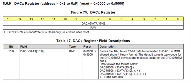
// 3. Write midscale (0x8000) to all 8 DAC channels (0x08–0x0F)

uint16_t midscale = 0x8000;

for (uint8_t ch = 0; ch < 8; ch++) {

spi_write_reg(fd, REG_DAC_BASE + ch, midscale);

}

// 4. Trigger LDAC update via software 

spi_write_reg(fd, REG_TRIGGER, 0x0010); // set LDAC to 1 4 th bit in reg 0x05

printf("All 8 channels updated to midscale (0x8000) with ×2 gain.\n");

printf("Expected VOUT ≈ 2.5 V (for 2.5 V internal reference).\n");

close(fd);

return 0;

}


  • Hi Anjana,

    Can you confirm that the edge timing is correct for the DAC60508? Note that the DAC latches data on the falling edge of SCLK.  What is the state of the CLR pin?

  • Hi Paul,

    Thank you for your quick response.

    For the clarification we have made 10K pull up on the CLR pin so that the chip will exit the clear mode operation.

    Today we have tried few configuration which is as follows in below sequence:

    1. wrote CONFIG reg with value 0x0000
    2. SYNC register is written with value 0xFFFF
    3. GAIN register is written with value 0x0700  
    4. BRDCST register is written with 0x0FFF
    5. TRIGGER register is written with 0x0010

    with this above setting we see Channel 0 with 0.148V and channel 4 with 0.313V and no change in other channels.

    Could you please let us know the above setting are right?

    Also please share the CODE value that to be written to DAC register?

    #include <stdio.h>
    
    #include <stdint.h>
    
    #include <fcntl.h>
    
    #include <unistd.h>
    
    #include <sys/ioctl.h>
    
    #include <linux/spi/spidev.h>
    
    #define SPI_DEV     "/dev/spidev2.0"
    
    #define SPI_MODE    SPI_MODE_0
    
    #define SPI_SPEED   1000000  // 1 MHz
    
    #define SPI_BITS    8
    
    // DAC60508 Register Addresses
    
    #define REG_NOP             0x00
    
    #define REG_DEVICE_CONFIG   0x01
    
    #define REG_SYNC            0x02
    
    #define REG_CONFIG          0x03
    
    #define REG_GAIN            0x04
    
    #define REG_TRIGGER         0x05
    
    #define REG_BRDCAST         0x06
    
    #define REG_STATUS          0x07
    
    #define REG_DAC_BASE        0x08   // DAC0 = 0x08, DAC7 = 0x0F
    
    // Helper function: write 3 bytes over SPI
    
    static int spi_write_reg(int fd, uint8_t addr, uint16_t value)
    
    {
    
        uint8_t tx[3];
    
        tx[0] = addr;
    
        tx[1] = (value >> 8) & 0xFF;
    
        tx[2] = value & 0xFF;
        return write(fd, tx, 3);
    
    }
    
    int main(void)
    
    {
    
        int fd = open(SPI_DEV, O_RDWR);
    
        if (fd < 0) {
    
            perror("open SPI_DEV");
    
            return 1;
    
        }
    
        uint8_t mode = SPI_MODE;
    
        uint32_t speed = SPI_SPEED;
    
        uint8_t bits = SPI_BITS;
    
        ioctl(fd, SPI_IOC_WR_MODE, &mode);
    
        ioctl(fd, SPI_IOC_WR_BITS_PER_WORD, &bits);
    
        ioctl(fd, SPI_IOC_WR_MAX_SPEED_HZ, &speed);
    
        printf("Initializing DAC60508...\n");
    
        // 1. Enable internal reference (CONFIG = 0x03)
    
        spi_write_reg(fd, REG_CONFIG, 0x0000);
    
        usleep(10000); // 10 ms delay for reference to stabilize
    
       //2. Set the SYNC register (SYNC=0x2)
    
        spi_write_reg(fd, REG_SYNC, 0xFFFF);
    
        usleep(10000);
    
        // 3. Set gain = ×2 for all channels (GAIN = 0x04)
    
        spi_write_reg(fd, REG_GAIN, 0x0700);
        usleep(10000);
    
          // 4. Set the BRDCAST register (SYNC=0x6)
    
        //spi_write_reg(fd, REG_BRDCAST, 110011001100);
        spi_write_reg(fd, REG_BRDCAST, 0x0FFF);
        usleep(10000);
    
    
        // 4. Write midscale (0x8000) to all 8 DAC channels (0x08–0x0F)
    
        //uint16_t midscale = 110011001100; //0.8V
        uint16_t midscale = 0x08F5;
        for (uint8_t ch = 0; ch < 8; ch++) {
    
            spi_write_reg(fd, REG_DAC_BASE + ch, midscale);
    
        }
        // 5. Trigger LDAC update via software (TRIGGER = 0x05)
    
        //spi_write_reg(fd, REG_TRIGGER, 0x001F); // set LDAC to 1 4 th bit in reg 0x05
        spi_write_reg(fd, REG_TRIGGER, 0x0010); // set LDAC to 1 4 th bit in reg 0x05
        usleep(10000);
    
    
        printf("All 8 channels updated to midscale (0x0FFF) with ×2 gain.\n");
    
        printf("Expected VOUT ≈ 2.5 V (for 2.5 V internal reference).\n");
    
        close(fd);
    
        return 0;
    
    }
    

  • Hi Anjana,

    Can you confirm what VDD voltage you are using? 

    A good way to determine if you're communicating correctly is to try turning the reference on and off. If you can turn the reference off, that likely means there isn't an issue with your SPI commands. It would also be helpful to get a scope screenshot of your SPI commands so we know if you're latching on the falling edge of SCLK. Sometimes these weird values can occur if you're not latching on the falling edge.

    Thanks,
    Erin

  • Hi Erin,

    We are using a VDD voltage of 3.3V.

    Through software control writing register 0x3, we can successfully able to turn the reference voltage on and off.

    The oscilloscope measurements were taken with the following modifications applied to the previous DAC60508ZC.c
    application:

    • The Config register is set to 0x0000

    • The Broadcast register is set to 0x0FFF

    • A midscale value of 0x0800 is written to all the DAC channels

    • Writing to the SYNC, GAIN, and Trigger registers has been disabled

    • SPI mode has been changed from SPI_MODE_0 to SPI mode 1

    With these modifications, we are able to get an output of approximately 0.079V on all 8 channels, but we are not able to achieve the required voltage level.

    Kindly suggest any changes or improvements.

    For the oscilloscope measurements, the SPI CLK and data pins(MOSI) were probed.

    Attached below are the oscilloscope screenshots of the SPI commands captured with these changes.


    Thanks.

  • Hi Anjana,

    I think is see the issue here: the dac-data is always left justified.  So midscale is not 0x0800, it is 0x8000!

    The 4 right-most bits are "don't-care".  So if you write 0x0FFF, you are actually writing value 0x0FF for the 12-bit register.  0x0FF/0xFFF*1.25V = 0.078V

  • Hi,

    I am unclear about which DAC register I should write to in order for the voltage to read correctly on the input pin.

    Specifically: if I set the Broadcast register to 0x0FFF, should I leave it as is, or do I need to provide the required voltage on the DAC pins to the Broadcast register?

    Thanks.

  • YOu are not writing data correctly to either the Broadcast or the DAC-DATA register.  If you want the DAC output to be midscale, the correct value to write to the DAC input register or the broadcast register is 0x8000.  Fullscale would be 0xFFF0.  You need to left-shift the data 4 bits.

    Thanks,

    Paul