ADC3544: Problems with clock frequency for data acquisition

Part Number: ADC3544


Tool/software:

Hello, I am attempting to collect parallel complex decimated data from this device and run into a problem whenever I increase the clock frequency above 500kHz.I have posted some example output plots given the following constant parameters:

NCO Frequency: 500kHz

Input frequency: 503kHz

Decimation setting: 2

Resolution: 16-bit

Note that when I say clock frequency I mean the input clock to the +/- input to the ADC3544, not DCLKIN as I am not using the serial mapper, but instead the parallel DDR data on outputs 1-16. These are plots of only the in-phase component of the complex decimated data.

This first plot I am plotting with clock frequency = 500kHz

For this plot, I am plotting every 10th value with clock frequency = 500kHz

For this plot I changed to clock frequency = 550kHz and plotting every value (input waveform doesn't appear to make a difference)

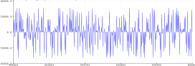
These plots make me think there is something wrong with the way the data is outputted or collected, but I am not sure what could cause it to work at clock input = 500kHz but not 550kHz. If I lower the clock frequency it still appears to work. Any help would be highly appreciated. Let me know if I can clarify anything.

Felipe.

  • Hi Felipe,

    What is the sampling rate you are using for your application and are you collecting this data from the TI evaluation board? Or your own design?

    It would also be good to get a list of reg writes used to configure the ADC so we can check it on our side.

    Please advise.

    Thanks,

    Rob

  • Hey Rob,

    Right now I am testing with the sampling rates said on the plots, so 500kHz, 500kHz, and 550kHz respectively. This data is being collected with my own design. Here are the register writes I am making:

    // Reset ADC
    writeToReg(0x00, 0x01);

    // Set output to parallel 16-bit DDR
    writeToReg(0x07, 0xA9); // 101 0 1 001
    writeToReg(0x13, 0x01); // 0000000 1
    delay(1);
    writeToReg(0x13, 0x0); // 0000000 0

    // Select 16-bit output
    writeToReg(0x1B, 0x08); // 0 0 001 000 for 16 (0x08)

    // Enable decimation filter
    writeToReg(0x24, 0x06); // 00 0 00 1 1 0

    // Set decimation by 2
    writeToReg(0x25, 1 << 4); // 0 001 0 00 0

    // Set NCO Frequency to 0.5MHz, f_out = 3903145718 (uint32)
    writeToReg(0x2A, f_out & 0xFF);
    writeToReg(0x2B, (f_out >> 8) & 0xFF);
    writeToReg(0x2C, (f_out >> 16) & 0xFF);
    writeToReg(0x2D, (f_out >> 24) & 0xFF);

    Thanks Rob,

    Felipe

  • Thanks Felipe for the details. We will look into this on the bench.

    You maybe in a mode that is not supported at low of a clock frequency.

    Are you open to other clock frequencies that support this specific mode?

    Regards,

    Rob

  • Hey Rob,

    My goal is to be able to sample at ~100MSPS and decimate by 16/32 bringing it down to 6.25 and 3.125MSPS. However, to test my device is capable of collecting data at these datarates I wanted to start at a lower bandwidth, i.e. starting at 500kHz decimated by 2 with complex decimation. The problem lies that when I try to increase the clock frequency above 500kHz it does not work any more.

    Thanks,

    Felipe

  • Hi Felipe,

    Please correct me if I have misunderstood, but this is what I think you are trying:

    Sample Frequency: 500kHz

    Resolution: 16 Bit

    Output interface: Parallel DDR

    Decimation: Complex by 2

    NCO Frequency: 500kHz

    Input Frequency: 503kHz

    If my understanding is correct, the configuration you are trying will not work. The NCO frequency is dependent on the sample frequency, and can be set to any frequency between -Fs/2 and Fs/2.

    Best,

    Luke Allen

  • Hey Luke,

    Yes I believe you are absolutely right. I have found at least one of the sources of error. When I write to register 0x07 (to select the output interface bit mapping) I write 0xA9 to select 16-bit DDR, however, when I try to load it in, once I write to the E-fuse 0x01 and then 0x00 the output goes bad. Do you know why this is the case?

  • Hello again Luke, I apologize but correct me if I'm wrong. Right now, I have my bit0 set to be on pin 38 and bit 15 on pin 20 of the ADC3544, however, there is a plot on Figure 8-37 that hints toward bit 0 being on pin 37 and bit 15 on pin 19. Have I mistakenly setup the pin outputs?

    Edit: this is for 16-bit DDR output.

    Thanks,

    Felipe

  • Hi Felipe,

    Yes, your pin configuration is incorrect. Please folow the mapping in Figure 8-37.

    Have you adjusted your NCO frequency to be between -Fs/2 and Fs/2?

    Best,

    Luke Allen