This thread has been locked.

If you have a related question, please click the "Ask a related question" button in the top right corner. The newly created question will be automatically linked to this question.

ADS1278-SP: Incorrect Power Sequence and Overcurrent

Part Number: ADS1278-SP
Other Parts Discussed in Thread: ADS1278

Good Afternoon,

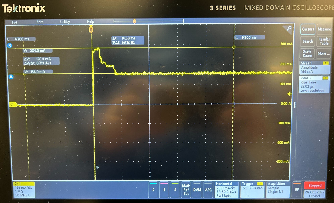
We have a critical application of an ADS1278-SP that was powered with the incorrect power sequence. IOVDD (2.5V) was applied before all other ADC voltages. This voltage was also applied to pin 15 (CLKDIV). Attached is a plot of the momentary input current to the device. It shows roughly 284mA for approximately 0.5ms before hitting the delayed source current limit of 150mA. I know the max momentary (how long is this?) current is listed as 100mA. Has any damage been done to this component, given all the information provided? What does the internal current path look like when only IOVDD is powered? 
scope.png

Please let me know if you have any questions for me.

Respectfully,

-Kevin   


IMG_8680

  • Hello Kevin

    First of all, the ADS1278-SP will not be damaged when using an incorrect power-up sequence.  We created an application note that discusses this topic in more detail.

    ADS1278-SP Power-On Reset Procedure

    We recommend the sequence specified in the datasheet for the following two reasons.

    1.  By not following the recommended power-up sequence, the device may not reset properly.  However, this can be easily corrected by asserting the SYNC pin after device power-on and data first appear.

    2.  When not following the recommended power-up sequence, all of the internal bias currents will default to maximum, which can result in as much as 2x the normal operating current on the AVDD supply.  This condition is not damaging to the device, and is not a concern as long as the power supply can deliver the increased current until proper reset.

    It is not clear to me if the above input current waveform is for IOVDD, or AVDD, or DVDD.  I would expect AVDD to reach about 200mA to 250mA, and then return to normal once all power supplies are up and the SYNC pin has been asserted.

    The ADS1278 can be damaged if one of the inputs has a voltage applied by more than 0.3V before the power supplies are up.  When this condition occurs, the 10mA continuous and 100mA 'momentary' rating now apply.  (The momentary is on the order of milliseconds to allow time for external ESD protection circuits to clamp.)  This situation can occur if the analog input amplifier is powered from a different supply than the ADS1278 AVDD supply, driving the analog inputs before the AVDD supply is up.

    Please confirm if the waveform above is for the IOVDD current.  If it is, then I would expect there is some other fault mode, such as driving the digital pins with an external controller (MCU, FPGA) before the IOVDD supply is powered up.

    Regards,
    Keith Nicholas
    Precision ADC Applications

  • Hey Keith - Thanks for the response. 

    The attached waveform is for IOVDD. It was the only voltage rail powered during this time. Below are a few follow-up questions:

    1 - In the datasheet, section 7.1, it lists the max digital input to ground as DVDD +0.3V. Can you confirm this is correct? Shouldn't this be IOVDD + 0.3V? Our design uses an IOVDD of 2.5V and a DVDD of 1.8V. 

    2 - When IOVDD (2.5V) is applied to our ADC, the CLKDIV also gets 2.5V. Does this condition trigger the 100mA max momentary rating for this digital input?

    3 - Are there any diodes between any of the ADC voltage rails, e.g. AVDD to IOVDD/DVDD, IOVDD to AVDD/DVDD, or DVDD to AVDD/IOVDD? 

    Let me know if you have any additional questions for me. I appreciate the support.

    Respectfully,

    -Kevin 

  • Hello Kevin,

    1.  This is a mistake in the datasheet.  All digital pins refer to IOVDD, and the digital inputs should remain in the range of -0.3V up to IOVDD+0.3V.  The commercial version of the ADS1278 datasheet correctly shows the ABS MAX specifications.  DVDD is only used for internal logic, and no external IO pins are referred to this supply voltage.

    2.  As long as the supply voltage for the logic gate driving the CLKDIV pin is the same 2.5V supply as the IOVDD supply voltage, then you will not have an issue with exceeding the voltage limits of -0.3V to IOVDD+0.3V.  However, if the logic gate supply is a different power supply, then this could violate the input voltage requirements during power-up.  You can easily confirm if this requirement is met by using a dual channel oscilloscope on power-up and measure both the CLKDIV and IOVDD pins.  Both voltages should ramp together assuming CLKDIV is driven high during power-up, and as long as the CLKDIV pin voltage is less than IOVDD+0.3V, you will not have any issues.

    3.  There are ESD protection diodes on all of the ADC digital and analog inputs.  There are no intentional diodes between the different supply rails (there are back to back diodes between the AGND and DGND pins), but since this is a monolithic IC, there will always be parasitic PN junctions that can be forward biased when the ABS MAX specs are exceeded and internally back-feed current into the other supplies.

    Even if you are exceeding the ABS MAX specs during power-up, it is not common for the device to go into a latch-up and draw high currents from the IOVDD supply, which is what appears to be occurring in your case.  There is one ABS MAX spec that is sensitive to latch-up if exceeded, and that is the AGND to DGND spec of -0.3V to +0.3V.

    I have seen customer boards that use a split ground plane between AGND and DGND, and then create a latch-up condition during some type of over-voltage or ESD event, where the ground plane voltages momentarily exceed these specs.  If you have split planes, you may also want to measure using a scope during powerup the AGND to DGND difference near the ADC package to see if there are any transients.

    QUESTIONS:

    • Does the ADC require a power cycle to clear the high current condition, or can you recover normal operation once all supplies are up and SYNC pin has been asserted?
    • Are you using a single ground plane, or a split ground plane that is connected together some distance away from the ADC package?
    • Does the IOVDD voltage overshoot during power-up and exceed the ABS MAX spec of 3.6V?  This could also cause a latch-up condition.

    Regards,
    Keith

  • Hey Keith,

    We have AGND and DGND tied together at the ADC. We ran the power up test again with only IOVDD and CLKDIV (2.5V, same supply) applied to the ADC. We see the same behavior. I attached a longer scope capture that shows the initial current spike, power supply limit at 150mA, and OCP shutdown. When we clear the OCP, we notice ~92mA constant current being drawn from our supply. I've also attached a scope capture of the voltage which does not show any overshoot of the 2.5V input into the ADC. 

    Answers to questions:

    • Does the ADC require a power cycle to clear the high current condition, or can you recover normal operation once all supplies are up and SYNC pin has been asserted?
      • Our supply trips for overcurrent (set to 150mA). When we clear the OCP, we see a steady 92mA being drawn from the supply (<2mA with IOVDD off). We have no tried anything with the SYNC pin at this time. 
    • Are you using a single ground plane, or a split ground plane that is connected together some distance away from the ADC package?
      • My understanding is we have a single ground plane that is split in some parts but everything is tied together close to the ADC. 
    • Does the IOVDD voltage overshoot during power-up and exceed the ABS MAX spec of 3.6V?  This could also cause a latch-up condition.
      • It does not appear to overshoot based on our measurements.

    Additional questions:

    1 - Would the momentary spike of ~280mA cause any degradation to the device for <1ms? How about the 150mA for ~40ms? And lastly, 90mA continuous? We are trying to assess whether this current draw is acceptable or if the part has been degraded to a point where it needs replacing. 

    2 - Are there any other conditions that you are aware of that could be causing the latch-up? 

  • Hello Kevin,

    The IOVDD supply should not exceed the datasheet specs of 1.5mA, even when not following the recommended power-up sequence.  There will be a momentary high current draw during power-up to charge up any internal or external capacitance on the IOVDD supply, but with a current limit of 150mA, this spike in current should be under 1 microsecond.

    Based on the information you have provided, it does appear the ADC is already damaged.  Since the ADC spikes at 280mA on power-up, and then the power supply current limits at 150mA, and then eventually you are able to get it to remain powered but with a steady current draw of 92mA, exceeding the 1.5mA max spec by quite a bit, points to a damaged device.

    As I had mentioned before, the power-sequence would not cause any damage, but it does appear something occurred in your system or during assembly that damaged the ADC.

    Answers to your questions:

    1.  The momentary spike is likely due to the ADC already being damaged from a previous event.

    2.  How is power applied to the ADS1278 in your system?  Is it powered from a linear or switching regulator, or is the power 'hard switched' using a MOSFET switch or some other mechanism in the system?  An extremely fast switch can cause ringing on the power supply rail due to any parasitic inductance on the supply line.  In some cases, this could cause high enough voltage overshoot to exceed the ABS max specs of the device and potentially damage it.

    Regards,
    Keith