ADS131E04: Unable to Read ID Register (0x00) on ADS131E04 via SPI

Part Number: ADS131E04


Hi, 
I am interfacing the ADS131E04 with my MCU through SPI. I’m following the startup sequence as per the datasheet:
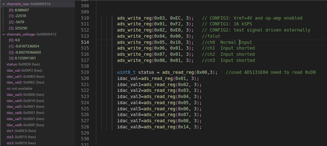
Sent RESET (0x06) command
Waited for 100 ms
Sent SDATAC (0x11) command to stop continuous data mode
Attempted to read the ID register (0x00)
However, I always read back 0x00 instead of the expected 0xD0 (for ADS131E04).
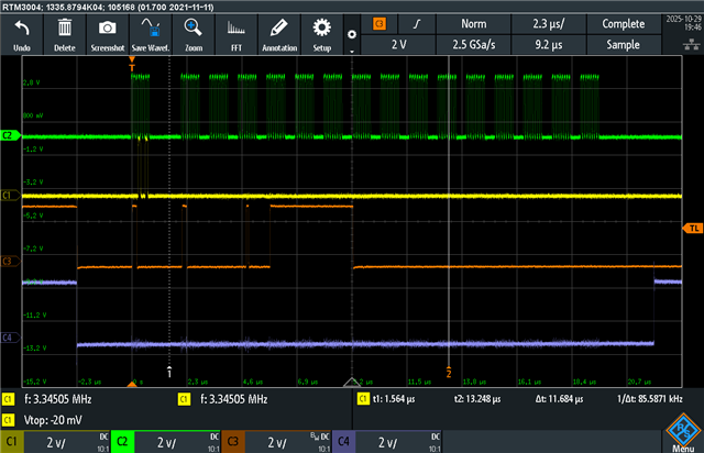
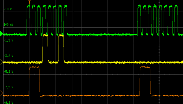
The SPI lines and MOSI data appear correct on the oscilloscope, and the first byte is transmitted properly.
Additional observations:
The MOSI first byte reflects the D0 data (both in the first and third bytes).
Sometimes, the correct 0xD0 pattern appears, but not consistently.
We tried running in all SPI modes (0 to 3), but the result remains the same.
Questions:
Is the WAKEUP (0x02) command mandatory before sending SDATAC and reading the ID register after power-up or reset?
What is the recommended delay after WAKEUP before register access?
Could improper VCAP capacitor values cause unstable SPI communication or ID read failures?
Are the VCAP, AVDD, and AVSS capacitor values required to exactly match the datasheet / EVM kit recommendations?
(Currently using either 1 µF and 10 µF capacitors for all rails.)


VCAP pins: Connected with 1 µF or 10 µF capacitors (need clarification if exact matching is mandatory).
SPI setup details:
SPI clock: 10 MHz
Verified correct MOSI data on oscilloscope
Thanks in advance for your support and guidance.

Thanks,
Manikandan V

  • Hi Manikandan V,

    Welcome to TI E2E forum.

    WAKEUP (0x02) command is not mandatory for reading registers.

    The VCAP pins are analog pins so the value of the capacitors on those pins do not affect SPI communication, however we strongly recommend to follow up ADS131E04 datasheet and use the same capacitors on the VCAP and AVDD pins for achieving the best performance.

    The RREG command is a multi-byte command, there are SCLK rate restrictions depending on how the SCLKs are issued to meet the tSDECODE timing as stated in 9.5.3.1 Sending Multibyte Commands section in ADS131E04 datasheet

     The ADS131E0x serial interface decodes commands in bytes and requires 4 tCLK cycles to decode and execute each command. Therefore, when sending multi-byte commands (such as RREG or WREG), a 4 tCLK period must separate the end of one byte (or command) and the next. Assuming CLK is 2.048 MHz, then tSDECODE (4 tCLK) is 1.96 µs. When SCLK is 10 MHz, one byte can be transferred in 0.8 µs. This byte transfer time does not meet the tSDECODE specification; therefore, a delay of 1.16 µs (1.96 µs – 0.8 µs) must be inserted after the first byte and before the second byte.

    Another alternative option is to reduce your SCLK frequency for reading or writing register during the configuration. If SCLK is 4 MHz, one byte is transferred in 2 µs. Because this transfer time exceeds the tSDECODE specification (2 µs > 1.96 µs), the processor can send subsequent bytes without delay. After you complete the configuration, you can set the SCLK frequency to a high frequency, the maximum SCLK frequency of ADS131E04 is 20MHz at 3.3V DVDD.

    When the device is in read data continuous mode, an SDATAC command must be issued before the RREG command can be issued.

    BR,

    Dale

  • Hi Dale LI,

    Thanks for your response,

    Initially, I was unable to read the correct register values, but after adding a 2 µs delay between two SPI bytes, I’m now able to successfully read the ID register (0xD0) and verify all written register values correctly using RREG commands.
    whenever i try to write or read data,MISO is responding to the 1st BYTE of the clk itself but  i receive the proper data in the expected clk byte also
    However, I’m facing an issue where CH0 always reads full-scale (0x7FFFFF), even when applying a valid DC input. Other channels return 0x000000.

    Test Setup

    Device: ADS131E04

    AVDD / AVSS: 5 V / 0 V

    DVDD: 3.3 V

    SPI Clock: 10 MHz (MODE0)

    VREFP–VREFN: Internal 4 V reference

    Gain: 1 (Full-scale range = ±4 V)

    Input:

    AIN0P → +1 V DC 

    AIN0N → GND (internal reference buffer connected 2.5V )

    Register Setup Sequence:
    ads_send_command(RESET); // 0x06
    DELAY_US(200);
    ads_send_command(SDATAC); // 0x11, Stop continuous read

    ads_write_reg(CONFIG3, 0xEC); // Internal reference buffer, op-amp enabled
    ads_write_reg(CONFIG1, 0xF2); // 16kSPS, CLK settings
    ads_write_reg(CONFIG2, 0xE0); // Internal reference enable, test signal disabled
    ads_write_reg(CONFIG4, 0x00); // Default
    ads_write_reg(CH0_CFG, 0x10); // CH0 = normal input
    ads_write_reg(CH1_CFG, 0x80); // CH1 powered down
    ads_write_reg(CH2_CFG, 0x80); // CH2 powered down
    ads_write_reg(CH3_CFG, 0x80); // CH3 powered down

    // Read the ID register (returns 0xD0 correctly)

    ads_send_command(START); // 0x08
    DELAY_US(1000);

    ads131e04_read_all_channels(channels_raw);

    Observation

    CH0 output is always 0x7FFFFF (full scale).

    CH1–CH3 output are 0x000000.


    Question

    Could you please suggest possible causes for the ADC reading full-scale values even with a valid analog input (1 V DC)?

    attached the clk,mosi,miso,cs waveforms,


    Is this early MISO activity (on the first byte) expected behavior from the ADS131E04?


    As shown in the waveform, the first status byte (0xC0) appears both during the first and second clock byte cycles. Ideally, it should appear only during the second clock byte, but it seems to be duplicated or shifted early on MISO.

    refer the below image,


    Please let me know if need any other details to debug the issues. 

    Thanks, 
    Saravana kumar M


  • Hi TI Team,

    We’re currently facing a bottleneck in our project due to this issue, and it’s blocking our progress. We’ve tried multiple approaches but are still unable to resolve it. Kindly help us to identify the root cause and provide guidance to resolve this at the earliest.

    Few Additional Details about the issue:

    We are following the voltage-sensing topology shown below — the negative input is biased at 2.5 V using the internally generated OPAMP_REF.

    We are feeding a 1V DC input to Channel 1, but the ADC output always shows a maximum hexadecimal value or some random value when reading the data.

    Please refer to the attached image for our connection topology (Figure 58: Simplified Current-Sensing Connections).

    Your timely support will be greatly appreciated.


    Thanks & Regards,
    Manikandan V

  • Hi Manikandan,

    I am really sorry that we are unresponsive this week. The application experts for this device are all out of the office this week.

    Your SPI communication looks correct to me. You can simply disregard the first byte on MISO while you are transmitting the RDATA command on MOSI. The first byte will always be (0xC0 + FAULT_STATP[7:4]). The important data starts with byte two on MISO, again with (0xC0 + FAULT_STATP[7:4]).

    The channels which are powered down always read 0x000000. That is correct.

    Why channel 0 reads 0x7FFFFF is not clear to me yet either. As a first debugging step I suggest to set MUX0[2:0] = 001b. This will short the positive and negative analog inputs to mid-supply internally. You should then read a value close to 0V. Please try that and report back.

    Regards,
    Joachim Wuerker

  • Hi Joachim,

    Thank you for your response and guidance.

    As suggested, I configured the device for the internal short test by setting MUX0[2:0] = 001b. After enabling this configuration, the output values are now reading close to zero across all channels, as expected.

    I’ve attached the measurement results and the configuration snapshot for your reference.

    Please check and let me know if there are any additional checks or configurations you would recommend next.

    Thanks and regards,
    Manikandan V

  • Hi Manikandan,

    thanks a lot for performing this test. It looks like the ADCs are converting properly and you can read the conversion data.
    Which register bits do your "status = 0x00D0" refer to?

    As a next step you can apply a known signal on the inputs again. I suggest to start with something simple. The device does not support single-ended measurements where the negative analog input is connected to AVSS, but for debugging purposes we can use that. Means connect INxN = AVSS and for example INxP = 1V. Don't drive the INxN input with the buffer or anything to level-shift it for now. You should read a value slightly less than 1V in this case.

    If this works, then we just need to find out what is wrong with your circuit implementation according to Fig. 58.

    Regards,
    Joachim Wuerker

  • Hi Joachim Wuerker, 

    The value status = 0x00D0 refers to the ID Control Register (address 0x00) of the ADS131E04.

    For the next step, I connected INxP = 1 V DC and INxN = GND as suggested. However, I’m mostly getting the full-scale output (0x7FFFFF or 8388607 in decimal), though occasionally I observe some fluctuating or floating values instead.
    Thanks, 
    MANIKANDAN V
  • Hi Manikandan,

    that is very weird. Can you confirm you are not connecting anything else to the channel 0 inputs besides the 1V signal on AIN0P and GND to AIN0N?
    Have you confirmed the voltages on both pins with a DMM?
    Previously you mentioned "AIN0N → GND (internal reference buffer connected 2.5V)"

    Have you tried any of the other channels?

    Regards,
    Joachim Wuerker

  • Hi Joachim Wuerker,

    Yes, the connections are correct. We are applying approximately 0.999 V on AIN0P, with AIN0N connected to GND.

    When measured using a DMM between AIN0P–GND and AIN0N–GND, the voltage fluctuates between 1.5 V and 1.8 V, eventually stabilizing around 1.8 V. Currently, there is no internal reference buffer connected to AIN0N, and the internal OPAMP_ buffer is disabled.
    We also observed the same behaviour on other channels during testing.

    In my configuration, VREF = 4 V and gain = 1. However, the ADC output appears to saturate when the input voltage exceeds approximately 250 mV, which does not align with the expected ±4 V full-scale range at gain = 1.

    Additionally, the ADC counts fluctuate by about ±30,000 across all tested voltage levels.

    Below are the measured results for different DC input levels:


    VREF = 4 V, GAIN = 1

    Analog Input (mV) Raw Data Calculated Voltage (V)
    10 313060 0.1493
    20 668230 0.3186
    30 1008030 0.4807
    40 1327500 0.6330
    50 1738340 0.8289
    60 2038880 0.9722
    70 2355530 1.1232
    80 2559000 1.2202
    90 2906820 1.3861
    100 3153780 1.5038
    110 3642070 1.7367
    120 3973280 1.8946
    130 4276090 2.0390
    140 4604960 2.1958
    150 5236250 2.4968
    160 5647540 2.6930
    170 5988420 2.8555
    180 6319020 3.0131
    190 6665440 3.1783
    200 7045520 3.3596
    210 7423770 3.5399
    220 7735600 3.6886
    230 8072240 3.8491
    240 8388607 4.0000
    250 8388607 4.0000

    VREF = 2.4 V, GAIN = 1

    Analog Input (mV) Raw Data Calculated Voltage (V)
    10 656200 0.1877
    20 1611970 0.4612
    30 2413290 0.6904
    40 3408840 0.9753
    50 4036580 1.1549
    60 5057570 1.4470
    70 5770360 1.6509
    80 6298850 1.8021
    90 7089670 2.0284
    100 7576480 2.1676
    110 8221250 2.3521
    120–250 8388607 2.4000 (saturated)

    Please let us know whether this can occur due to any connection issues or capacitor placements in the Analog power and VCap pins ? 


    Thanks and regards,

    Manikandan V

  • Hi Manikandan,

    I think this would be a good time to review your schematic for any issues as it is quite puzzling what is happening here. Could you please share the schematic with me for review?

    From the output codes it looks like as if a gain = 16 is used.
    I do currently not have a good explanation for why you would measure 1.5V to 1.8V with the DMM on AIN0P.

    Have you tried any measurements without configuring the ADS131E04 at all? Just use it in its default register configuration?
    You might at least have to set PDB_REFBUF = 1b though when using the internal VREF.

    Regards,
    Joachim Wuerker

  • Hi Joachim Wuerker,

    Yes, you are correct — the issue was due to a dry solder joint on the VREFN pin connection to ground. After re-soldering, the ADC output counts now respond correctly according to the input voltage.

    Below are the test observations for input voltages from 0 V to 4 V. The measured ADC counts closely follow the expected values, confirming that the reference and input circuitry are functioning properly.

    From the data, we observed a variation of approximately 5000–7000 counts, corresponding to about 3 mV offset.

    Could you please confirm if this level of deviation is normal for the ADS131E04 device, or if there are ways to further optimize/reduce this error?

    Thank you for your continued guidance and support.

        FORMULA Diff btw expected and actual VOLATGE Diff of count in VOLT(mV)
    S.No Analog Voltage(V) EXPECTED ACTUAL      
      0 – 4 V Adc counts after formula Rounding  Off Adc_count      
                   
                   
    1 0.005 10485.75875 10486 2880 -7606 0.001373291 -3.63
    2 0.006 12582.9105 12583 4060 -8523 0.001935959 -4.06
    3 0.007 14680.06225 14680 7730 -6950 0.003685952 -3.31
    4 0.008 16777.214 16777 8690 -8087 0.004143715 -3.86
    5 0.009 18874.36575 18874 10960 -7914 0.005226136 -3.77
    6 0.01 20971.5175 20972 12710 -8262 0.006060601 -3.94
    7 0.02 41943.035 41943 34260 -7683 0.016336443 -3.66
    8 0.03 62914.5525 62915 55140 -7775 0.026292804 -3.71
    9 0.04 83886.07 83886 76570 -7316 0.036511426 -3.49
    10 0.05 104857.5875 104858 97430 -7428 0.04645825 -3.54
    11 0.06 125829.105 125829 119140 -6689 0.056810386 -3.19
    12 0.07 146800.6225 146801 139760 -7041 0.066642769 -3.36
    13 0.08 167772.14 167772 160980 -6792 0.076761255 -3.24
    14 0.09 188743.6575 188744 181420 -7324 0.086507808 -3.49
    15 0.1 209715.175 209715 202720 -6995 0.09666444 -3.34
    16 0.2 419430.35 419430 412850 -6580 0.196862244 -3.14
    17 0.3 629145.525 629146 621410 -7736 0.296311414 -3.69
    18 0.4 838860.7 838861 832160 -6701 0.396804857 -3.20
    19 0.5 1048575.875 1048576 1042490 -6086 0.497098028 -2.90
    20 0.6 1258291.05 1258291 1251560 -6731 0.596790385 -3.21
    21 0.7 1468006.225 1468006 1461760 -6246 0.697021567 -2.98
    22 0.8 1677721.4 1677721 1671450 -6271 0.797009563 -2.99
    23 0.9 1887436.575 1887437 1881130 -6307 0.89699279 -3.01
    24 1 2097151.75 2097152 2091490 -5662 0.997300267 -2.70
    25 1.5 3145727.625 3145728 3140030 -5698 1.49728316 -2.72
    26 2 4194303.5 4194304 4187830 -6474 1.996913194 -3.09
    28 2.5 5242879.375 5242879 5235790 -7089 2.496619522 -3.38
    29 3 6291455.25 6291455 6284840 -6615 2.996845603 -3.15
    30 3.5 7340031.125 7340031 7333070 -6961 3.496680677 -3.32
    31 4 8388607 8388607 8381470 -7137 3.996596813 -3.40

    Additionally, we need a few clarifications regarding timing optimization and sampling behavior of the ADC. We’ll share our observed timing data and follow up with further details soon.

    Best regards,
    Manikandan V

  • Hi Manikandan,

    thanks a lot for the positive news. I am glad you found the issue on the PCB.

    How did you apply the 0V to 4V signal?
    As mentioned previously, the device does not allow single-ended measurements where INxN is connected to GND. I just had you use this configuration for debugging purposes. If you used a single-ended measurement, then I am not surprised to see this offset/non-linearity.

    When using Gain=1 you will have to level shift the signal at least by 300mV. Means you can set INxN = 300mV for example and then sweep INxP from 300mV to 4.3V to create a differential input signal ranging from 0V to 4V.

    Beyond that, you can implement a self-offset calibration by leveraging the internal short connection you tested previously.
    And then you could also implement a system gain calibration to get rid of the initial gain error and VREF inaccuracy.

    Regards,
    Joachim Wuerker 

  • Hi Joachim Wuerker,

    We are currently providing the input signal from a Digilent Analog Discovery 2 device using crocodile clips.
    At the moment, the IN1N pin is connected to the Digilent negative output (GND), and the IN1P pin is connected to the positive terminal of the Digilent device.

    I’m still not completely clear about the DC bias requirement on the IN1N pin — could you please explain this in a bit more detail?

    As suggested, we will proceed with implementing the device self-offset and gain calibration routines.

    Below are the details of our input signal conditions:

    1. –125 mV to +250 mV DC signal — with step increments of 2 mV.

    2. 0 V to 4 V, 400 Hz sine wave — with step increments of 50 mV.

      • The sine wave is single-ended and positively biased.

      • Our original source signal is a ±2 V sine wave, which we bias through a differential op-amp stage (with reference voltage) to create a 0–4 V swing before feeding it into the ADC.

      • This setup was originally designed for a single-ended ADC, and the PCB is already fabricated. We later switched to this simultaneous sampling device to optimize acquisition timing.

    We have approximately 25 analog input channels with different voltage scaling configurations. Each channel is conditioned to fall within the ADC’s readable range.
    Our lowest input signal amplitude is 2 mV, and we’d like the ADC to be able to accurately capture such small levels.

    Could you please suggest the recommended configuration or best approach for using the ADS131E04 to handle these signal conditions effectively?

    Thank you once again for your valuable support and guidance.

    Below is the example image of our ADC input : 

    Best regards,
    Manikandan V

  • Hi Manikandan,

    the common-mode input voltage range limitation is due to the PGA that is used in front of each ADC channel. As with any traditional instrumentation amplifier, the PGA requires a certain common-mode input voltage to operate. Equation 4 in the datasheet represents this limitation. It is always a bit hard to interpret this equation unfortunately. For gain = 1, all the formula is saying is that both INxP and INxN need at least 300mV headroom from either supply rail at all times. If that headroom is not met, then the PGA outputs would saturate leading to non-linear behavior.

    One solution for your 0-4V sine wave signal measurement would be to level shift the whole signal (both on IN1N and IN1P) by 300mV to 500mV. Alternatively, you could connect IN1N to 2V, and then attenuate the sine wave signal on INxP so it swings 2V +/-1.7V. Having IN1N = 2.5V and IN1P swing 2.5V +/-2V would work as well. Lastly, you could also operate the ADS131E04 with a bipolar analog supply (+/-2.5V). That way you could directly measure the +/-2V sine wave signal.

    Regarding your DC signal. Please note that you cannot measure signals below GND when using a unipolar analog supply.

    Regards,
    Joachim Wuerker