


Part Number: ADS1299-4
Other Parts Discussed in Thread: ADS1299
Hello,
I am designing a single-supply EEG device using the ADS1299-4, and Nordic nRF52840 BLE and I’m facing an issue related to the SRB1 and channel negative inputs (INNx) ( or may be any other problem that couldn't observe) connection in referential montage mode.
The device is powered by a battery— 5 V of analog supply and 3.3 V for digital supply. I am using the internal reference of the ADS1299, and it seems to be working correctly.
Hardware Overview
- ADC: ADS1299-4
- Supply: Single 5 V analog, 3.3 V digital
- Reference: Internal reference enabled (buffer ON)
- Configuration: Referential montage, 4 channels (4 leads), 1 lead for SRB1, and 1 lead for BIASOUT
- Input: Each channel has a first-order RC filter
- Verified voltages (all measured correctly):
- VREF = VREFP – VREFN
- VCAP1 = AVSS + 1.2 V
- VCAP2 = (AVDD + AVSS) / 2
- VCAP3 = AVDD + 1.9 V
- VCAP4 = AVSS + (VREFP + VREFN) / 2
Firmware Configuration
Below is the relevant initialization sequence:
ADS1299_write_register(CONFIG1, 0xD6);
ADS1299_write_register(CONFIG2, 0xC0);
ADS1299_write_register(CONFIG3, 0xEC);
ADS1299_write_register(CH1SET, 0x60);
ADS1299_write_register(CH2SET, 0x60);
ADS1299_write_register(CH3SET, 0x60);
ADS1299_write_register(CH4SET, 0x60);
ADS1299_write_register(BIAS_SENSP, 0x0F);
ADS1299_write_register(BIAS_SENSN, 0x0F);
ADS1299_write_register(MISC1, 0x20);
Channels 5–8 are powered down (0x81), and SPI communication works fine.
Reading the ID register returns 0x3C as expected.
Issue
According to the datasheet, the INN1–INN4 inputs should be internally shorted to SRB1 when SRB1 is enabled.
However, in my case this internal short doesn’t seem to function as expected.
Here are my observations:
- When I apply an input signal to channel 4, I can see the output on channel 1 and channel 3. and channel 2 and 4 are full of noise
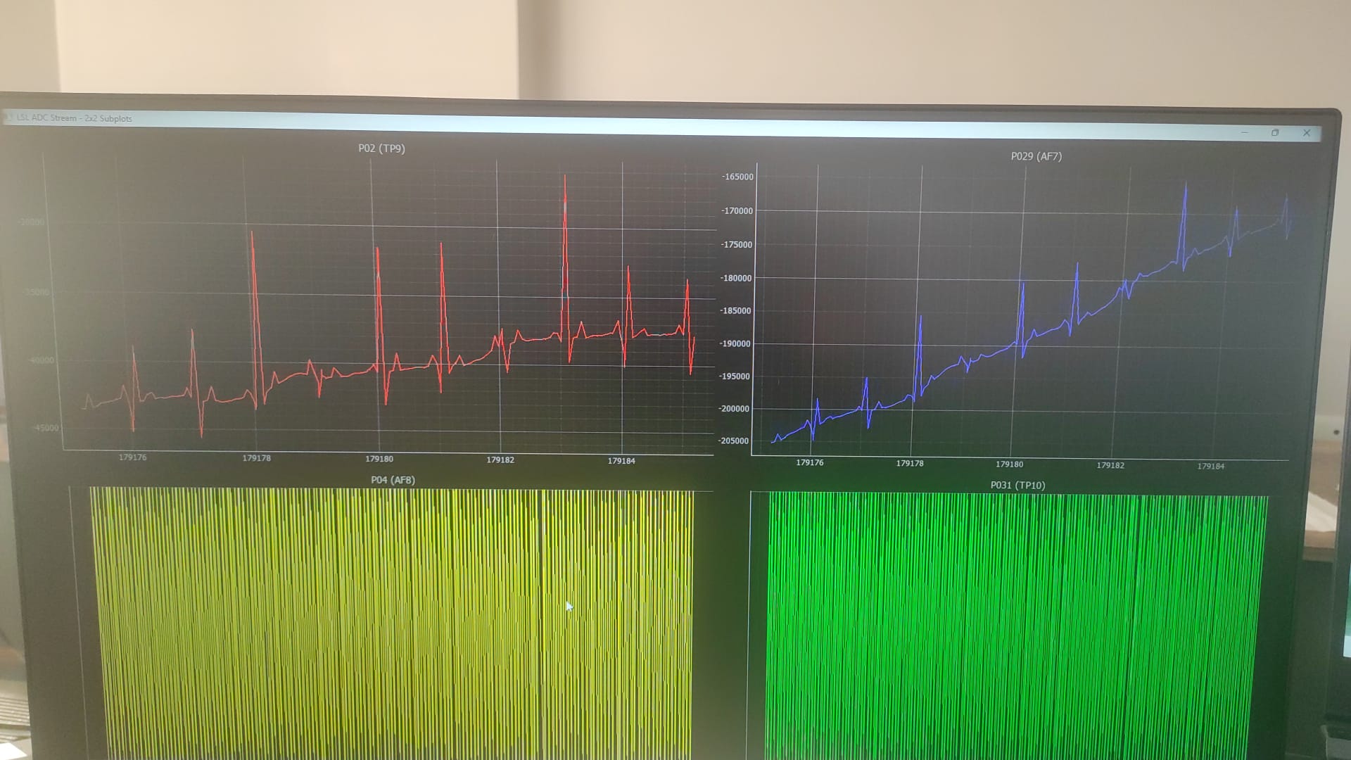
- When I apply an input signal to channel 1, no output is observed on any channel.
It seems that the SRB1 internal connection is not properly working or not being configured correctly.
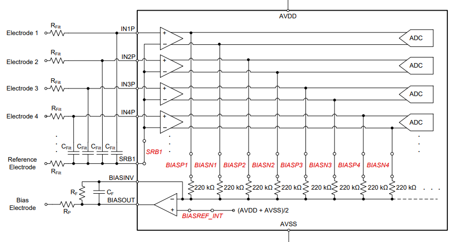
The design is exactly the same as schematic above.
Questions
- Could there be a configuration or register setting that prevents the internal short between SRB1 and INN1–4 from being established?
- Is my setting of
MISC1 = 0x20correct for enabling SRB1? - Do I also need to set any specific bits in each
CHnSETregister to connect INN lines to SRB1? - On the hardware side, should SRB1 be left floating (not tied to bias or reference) when used internally?
Any insights or debugging suggestions (e.g., register dump comparison, internal mux test methods, or expected impedance measurements between SRB1 and INNx or any hardware rework) would be greatly appreciated.
I can share schematic snippets, PCB photos, or scope captures if needed.

