DAC39RF12EVM: Core Clock setting

Part Number: DAC39RF12EVM


Hi Team,

Posting on behalf of our customer.

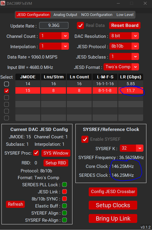
I am using the DAC39RF1xEVM GUI to setup the clocks and registers on the DAC39RF12EVM. When I follow the AMD JESD204C v4.3 LogiCORE IP Product Guide (PG242) specification document it says that for the JESD Protocol 8b10b the clock frequency should be the serial line rate divided by 40. When I try to setup a serial line rate of 11.7Gbps the Core Clock should be 292.5MHz, but your GUI seems to be setting it up as 146.25MHz. It’s essentially taking the line rate and dividing it by 80. Can you confirm that this is being setup correctly and that it will work with a Xilinx FPGA that is communicating the same line rate but operating with an FPGA clock of 292.5MHz?

image002.png

Regards,

Danilo

  • hey Danilo, 

    The GUI is setup to work with the generic JESD204C firmware we produce which uses a line-rate by 80 divider for 8b10b line encoding. Our custom JESD204B/C firmwares also use this. 

    The latest version of the GUI (version 3.2.0) includes API example scripts (within the the same folder as the executable) which will allow you to change the clock frequencies going to the FPGA. By default for all 16 bit modes the EVM accepts the DAC_CLK/16 as a reference clock. From there you can customize the LMK reference clock dividers be 2x higher than the default value used in the API examples. 

    You can change this line here to match your needs. 
    fpga_clk_divider = 66 if jesd_link_layer == dac39rf1x_enums.JESD_JENC_64B66B else 80

    to 

    fpga_clk_divider = 66 if jesd_link_layer == dac39rf1x_enums.JESD_JENC_64B66B else 40

    you can simply remove any of the FPGA setup code if you are not using our generic firmware. I would recommend setting up the clocks, stop at a debug point to setup the FPGA and from there setup the DAC, this will allow the script to get proper lane arrivals and set the RBD accordingly. 

    Regards, 

    Matt