This thread has been locked.

If you have a related question, please click the "Ask a related question" button in the top right corner. The newly created question will be automatically linked to this question.

DAC80501: DAC80501 – Linearity Issue at Low Output Range

Part Number: DAC80501

Dear Sir or Madam,

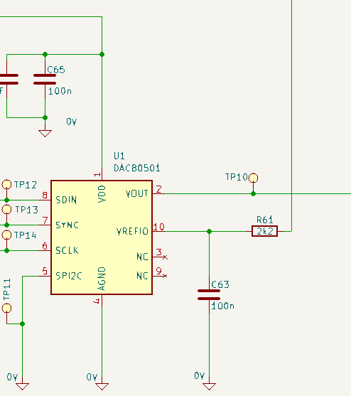
We are using your DAC80501 with an external reference of 4.096 V. Please find the schematic attached.

As you can see from the attached waveform plots, there appears to be a linearity issue in the range between 0.0 V and 0.02 V. As a simple example, we programmed a triangular waveform oscillating between 0 V and 62 mV. Below 10 mV, the waveform is clearly non-linear. This behavior does not occur at the upper transition point.

When we apply an offset of approximately 20 mV to the entire signal, these non-linearities disappear entirely. This confirms that the issue is strictly limited to the very bottom of the output range.

Based on the datasheet, we would expect significantly better linearity performance. This was also one of the main reasons we chose this device.

Question 1: Is there anything we may have overlooked in the datasheet, and is this behavior expected from the DAC?

Question 2: What can we do to improve the linearity in this low-voltage range?

Thank you very much and kind regards, Dan

Attachments:

  • Schematic

  • Distorted triangle waveform

  • Correct triangle waveform with offset

  • Distorted sine waveform

  • Correct sine waveform with offset

DAC80501_Schematics.pngTriangle_without_Offset_FAIL.pngTriangle_without_Offset_FAIL_2.pngTriangle_with_Offset_PASS.png

Sinus_without_Offset_FAIL.pngSinus_without_Offset_FAIL_2.pngSinus_with_Offset_PASS.png

  • Hi Dan,

    I think you are seeing some overdrive recovery of our output buffer.  Basically, a DAC has an output buffer that has the same limitations of any other amplifier, and in this case I think you are seeing some overdrive recovery issues.  All amplifiers have limited output ranges, with the best being "rail-to-rail".  Ours is not quite rail-to-rail output, and a combination of negative offset error is driving the amplifier to be less than 0V.  When this happens, parts of the output buffer saturate and cause delays when the input to the buffer becomes greater than the zero-scale error of the amplifier.  

    In our electrical characteristics, you see that we have a zero-scale error of a few mV, and that we specify our linearity only as low as code 256.  That is about 16mV in your configuration I believe.  

    This is mostly exhibited when you are generating a dynamic voltage like you are doing.  If you were doing a much slower rate, you would probably only notice the lowest few LSBs being an issue.  

    I recommend using a few LSB offset to prevent the DAC from reaching ~<2-3mV in normal operation if you need to keep this update rate.

    Thanks,

    Paul

  • Hi Paul,

    Thanks for your efforts in providing a quick response. I actually just now noticed the note (1) in the datasheet stating that linearity is only guaranteed from code 256 to 64511. We had overlooked that. Thank you for pointing it out.

    So we'll need to work with a small offset. At least now we know it's not an issue with our circuit, and we can move forward with the project.

    Kind regards, Dan