This thread has been locked.

If you have a related question, please click the "Ask a related question" button in the top right corner. The newly created question will be automatically linked to this question.

ADS7863A: Unexpected input (SDI) configuration

Part Number: ADS7863A

I want to convert 2 ADC readings simultaneously and read them back on a single line (OUTA on the ADS7863A). Based on the datasheet for this chip, I would like to use special mode 2 to send a single CONVST signal from my microcontroller and read the 2 conversions. I believe I'm sending the correct SDI (input to ADS7863A) configuration, but I only get a single conversion back on the output (first image attached). I have noticed that if I shift my SDI to the right by 1 bit (second image), then I get 2 conversions back on the output, but then my SDI configuration is in an unexpected state from my understanding of the datasheet.


I need to ask the ADC for 2 conversions on the single output very frequently so I would like to stick with special mode 2 so I don't have to worry about raising CONVST multiple times per read attempt.
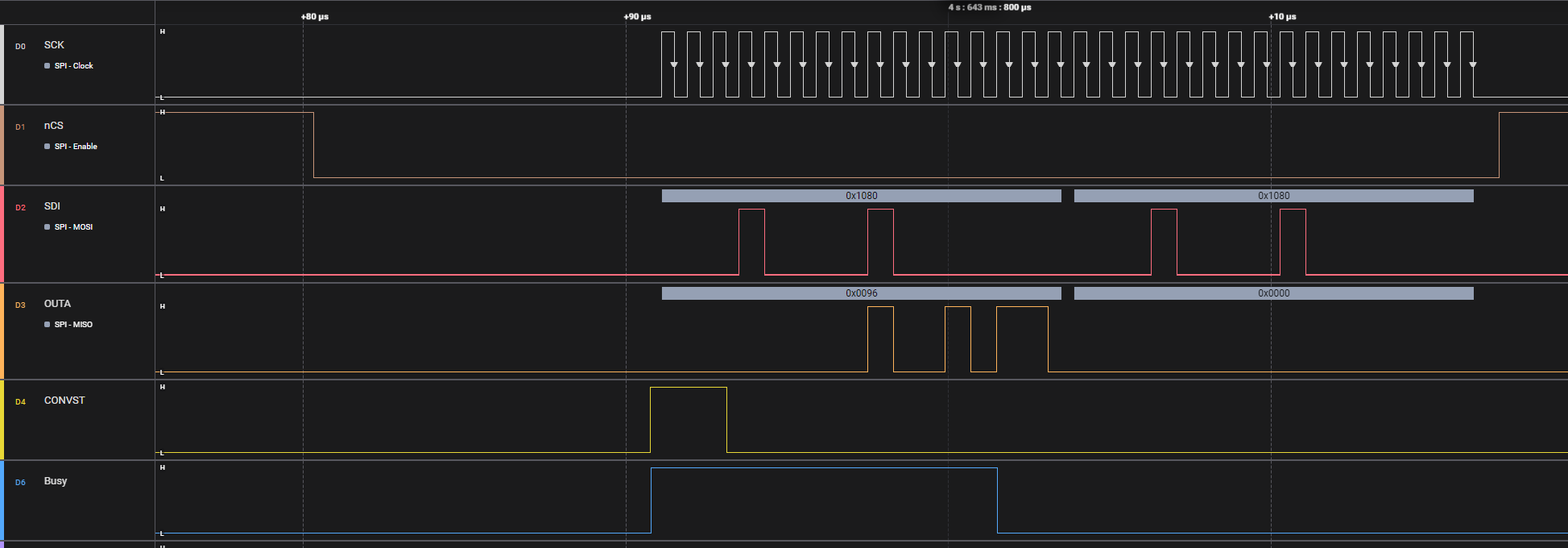
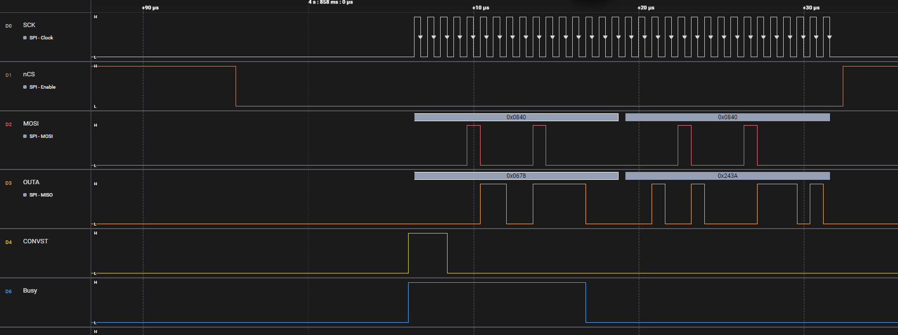
image.png

image.png

  • Hello Brendan, 

    Welcome to TI's E2E forum! Thank you for your question!

    Are your RD & CONVST shorted together?

    For writing to the device, the 1st falling edge of the CLOCK that in within the set-up and hold time of the RD timing parameters is what begins the SDI data transaction. After that 1st falling edge (if within the parameters) the next falling edge is when it will latch the data from the SDI, which why when you shift the data by one the device functions as intended. 

    Best regards, 

    Yolanda

  • RD and CONVST are shorted together.

    That makes sense now. Thank you

    I also interpreted the OUTA from the datasheet (special mode 2) to start with either 00 (for channel A) or 01 (for channel B), followed by 12 bits of data, and finally 2 trailing 0s for the full 16 bit output.

    Looking at my waveform with the information you just provided that doesn't seem to be the case. Can you clarify the structure of the output?

  • Hello Brendan, 

    You are correct in the interpretation of OUTA being {CH[16:15],Data[14:2].0s[1:0]} , where the CH bits would be 00 for CHA and 01 for CHB.

    From the waveform you shared, the one with the shifted data that actually output the data from both channels, it appears that it is actually coming out in the format mentioned. 

    In your waveform it reads 0x0840,0x0840 on SDI, which we know is shifted to right by 1 bit and the ADC is actually reading 0x1080, correct? 

    So if we do the same to the SDO data and shift the 0x0678,0x243A by 1 bit to the left, then the SDO that the ADC is actually outputting is 0x0CF0,0x4874.

    Then following the format {CH[16:15],Data[14:2].0s[1:0]}, for CHA = [16:15] = 00 and CHB = [16:15] = 01


    Could you adjust the logic decoding on the logic analyzer and confirm? Or would you share what the expected data out from each channel would be? 

    Best regards, 

    Yolanda 

  • That makes sense. I do see the correct structure now.

    In my case of doing 2, 16-bit reads (where I also update SDI), is the ADS7863A capable of outputting the data with 32 clock cycles without being shifted by 1 bit?

    Do I need to trigger CONVST/RD at a different time?

    Or do I need to use 33 clock pulses, where the 1st pulse is what begins the SDI transaction and the remaining 32 bits will output the unshifted data?

  • Hello Brendan, 

    Because of the CONVST and RD functionality the 33 clock with bit shift for the data capture would be the best approach. 

    The extra clock could only be needed during the 1st conversion. It could be timed so that the 33rd clock is the 0 clock of the 2nd conversion recovering the 32 clock cycle. 

    Best regards, 

    Yolanda