


1. Fault phenomenon
Our company's product AD collects three channels of UFH (CH2), UFS(CH3), and UFX(CH4) at a given 5V. At -20℃, the collected results are CH2=2.913V, CH3=2.531V, and CH4=2.532V. This faulty sample accounts for approximately 70% of this batch. The non-faulty products were collected normally at -40℃.
Our company's products use the ADS8568SPM chips from the 2018 and 2023 batches, both of which have this problem.

Abnormal AD data waveform at -20℃ (should be 0x7fff, actual AD output 0x4079)
Normal AD data waveform at -20℃ at 5V (0x7fff)
2.AD circuit schematic diagram (ADS8568SPM)


Hardware configuration mode, 2x REF, adopts internal reference REF=2.5V, SPI communication, power supply HVDD=+12V, HVSS=-12V, AVDD = DVDD = 5V.
3. Preliminary investigation results show that the internal DAC output reference of the AD chip is abnormal at low temperatures
1) Abnormal reference voltage values during low-temperature screening
After investigation, it was found that the faulty sample product had abnormal REFA, REFB, REFC, REFD and REFIO when powered on at low temperature (-20℃), as shown in the following figure:

It is manifested as all reference voltage values not being 2.5V after power-on. The reference voltage anomaly measured in the above figure cannot be restored by setting the AD RESET pin high either. This leads to abnormal voltage values collected by all AD channels.
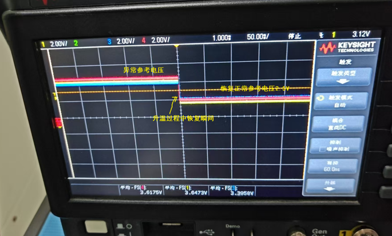
2) Inspection situation during the process of restoring to normal temperature
The above-mentioned faulty samples were restored to room temperature, and the reference voltage values were monitored in real time. It was found that during the temperature recovery process, all reference voltage values returned to the normal 2.5V during the heating process (the product was continuously powered on during this process without any operation).
3) Normal temperature inspection situation
After the power is on and stabilizes at room temperature and AD is reset, the reference voltage is correct, which is 2.5V, as shown in the following figure

However, at the moment of power-on, the reference voltage was abnormal at the moment of power-on, and then the chip's power-on self-reset (POR) was restored, as shown in the following figure.

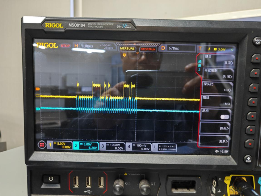
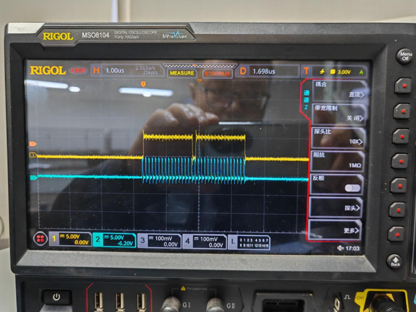
4) Power supply inspection
The yellow in the following figure shows the 5V power supply of AVDD and DVDD, the blue one is HVDD +12V, and the red one is HVSS -12V waveforms. The power supply waveforms are consistent at the moment of power-on, -20℃ and normal temperature. The power supply operates normally without jitter during the power-on process. We also adjusted the power-on sequence for troubleshooting, but the fault can still be reproduced at low temperatures. Therefore, this fault has nothing to do with the power supply.

