Part Number: ADS8689
In a new analog input board we use ADS8689IPW A/D converter.
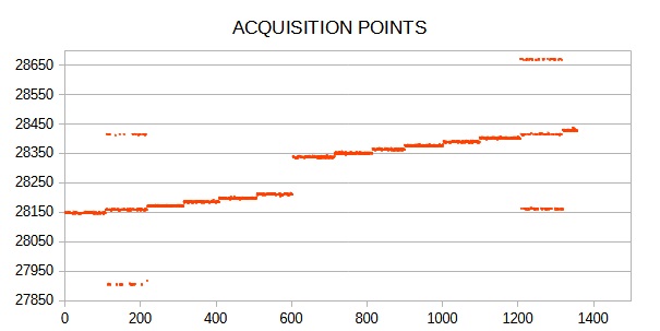
During debugging we noticed a strange behaviour of converted values: (only) at certain levels of input voltage the converted points have an everage value (the expected one, corrisponding to the converted voltage input), but also there are a lot of values at other two different and precise levels, both distant exactly ±256 points from the expected value. Apparently these values are wrong ones.
And this pattern occurs every 20mV (again corresponding to 256 points, because we use unipolar 5.12V input range). On every other input voltage level different from these 20mV multiples the conversion results are perfect and only have one well defined average value.
In our application the ADC has 5V single power supply and it uses internal voltage reference. The SPI signals are precisely managed by an FPGA, with conversion time 5us and acquisition time 75us, with communication at 2MHz and 16 bits frames. (Initial configuration is a "one-shot" 32 bits 0xD014_000B frame after power-on.)
We do not use RVS pin, but during debugging we verified that conversion time is always 1us, even during wrong result values. Besides, at wrong conversions we also verified that the wrong binary results effectively corrispond to SDO signal bits (that is SPI communication is ok).
During debugging with gradually excluded all others circuits external to the ADC. We by-passed analog input conditioning stages, finally connecting input source directly to the ADC (without noting differences in the problem). We verified the problem with different input voltage generators (Fluke 724 calibrator, FNIRSI SG-004A signal generator, simple linear power supply and even simple battery). We monitored power supply voltage without finding differences between good and bad conversions, and even replaced the original power supply from the board with an external DC lab one. We monitored voltage reference (and even disconnected all external high-impedance circuit) without finding differences between good and bad conversions.
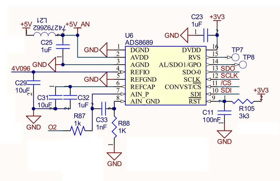
The ADC schematic is as from indications of its datasheet. On input pins, AIN_P and AIN_GND, there are 1kR series resistors and 1nF parallel capacitor.
Attached you find an image of approx 1300 conversion values at different input levels, and you can easily see the error values at two well-defined levels - 28160pts~2.2V and 28416pts~2.22V.
Attached you also find the schematic of ADC and an oscilloscope image of SPI frame.
What is the problem? Is it a known problem? How can it be solved (other than sw-averaging)?
Thanks, Roberto.