This thread has been locked.

If you have a related question, please click the "Ask a related question" button in the top right corner. The newly created question will be automatically linked to this question.

ADS9224REVM-PDK: Incorrect reading

Part Number: ADS9224REVM-PDK

Hi Experts,

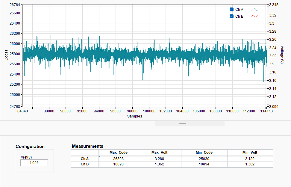
I have received the evaluation board , a day ago, and i tested the board by applying 3.3v (STM32 3v3) to JP2 and shunted J2. All other jumpers in the default configuration. I'm getting a maximum reading of 3.1V.

On a second try i got 3.288V. I want to understand why it is like that
evm_3.3_nov18.png

evm_3v3_stm.png

I have also made another set of reading using Keithley 2450 sourcemeter

ADS9224R EVM Keithley.zip 

Regards,

Marvin

  • Hello Marvin! 

    I am glad you are able to try out the ADS9224REVM! 

    At 1st glance I would say the STM32 3v3 source is quite noisy, which would make sense to me since it probably more of a digital supply or i might be prone to some noise from the USB. 

    And after looking at your Keithely readings, it appears like it is a lot less noisy than the STM32 3v3. 

    How are you connecting the DC source to the JP2 and how are you shunting J2?  Set-up can sometimes add noise too. 

    Since you are currently doing single ended DC measurements I would also recommend looking into:

    • Adding a bit of an offset on the REF/2 output 
    • the FDA negative supply, could you please let me know if JP7 is open as well as if JP8 is in [1:2] position 
    • **These suggestions are not too crucial since you are only going up to 3.3V, but its worth trying. 

    Best regards, 

    Yolanda

  • Hi Yolanda,

    I'm shunting J2 by closing the jumper cap. I connected the DC source using jumper wires with signal on JP2 and boards(STM32) ground connected to other header of J3. JP7 is closed and JP8 is in [1:2] position.

    Adding a bit of an offset on the REF/2 output - i will try that and let you know

  • Hello Marvin, 

    The reason why I  asked about JP2 and J2 is because they aren't purposely named/numbered, the In+ of THS is J2/JP1 and the In- is J3/JP2. I'm sure you are using it as intended, but I wanted to put it out there just in case. 

    Having the DC input on JP2[1]/J3 and shunting J2/JP1 makes perfect sense.  I was also curious if your DC input was through the header JP2[1] or J3.  JP2[1] should work well, but J3 would be preferable due to the SMA shielding and possibly helping to reduce the external noise input. .

    For the shunting, going through JP1 would be easiest but there are some SMA shunts too, this is less of a concern. 

    Let me know how it goes with the added offset!

    Best regards, 

    Yolanda

  • Hi Yolanda,

    Right now I don't have a SMA connector with me. I will try it later, In the mean time I want to talk to you about another issue.
    Can I program the eval board, while being plugged with the PHI controller board. I have soldered the testpoints for SPI, I have shunted the extCONVST pin, with the phi controller board connected, I sent a write command to set PROTOCOL_CFG to a value 3, then i sent a read command to read the same register, then again initiate spi to read the values (please confirm whether im doing this right, like for read operation it is not simulataneous transmit and recieve). I'm not getting a response. I have verified that commands are being sent with help of logic analyzer. If i need to separately power, can i use my STM32 boards 3v3 and 5v.

    Thanks!

    Marvin

  • Hello Marvin, 

    Apologies for the delay, I was out of office for some time. 

    You should not connect a different controller while the PHI is connected.  This would cause both the PHI and the STM to drive the lines and it could damage either of the controllers. 

    If you want to use the power or any other resources available from the PHI, I would recommend removing the 0Ω resistors and driving the digital lines with the STM32 after those. 

    If possible I would recommend using the STM32 power (EVM_REG_5V5/VA & DVDD) along with the digital lines. If a connector similar to the one on the EVM is possible great, other wise I would recommend connecting it via the 0Ω resistors for the digital lines or their respective test points. 

    Best regards, 

    Yolanda
