This thread has been locked.

If you have a related question, please click the "Ask a related question" button in the top right corner. The newly created question will be automatically linked to this question.

ADS9813: data offset

Part Number: ADS9813
Other Parts Discussed in Thread: , TSWDC155EVM

Dear all,

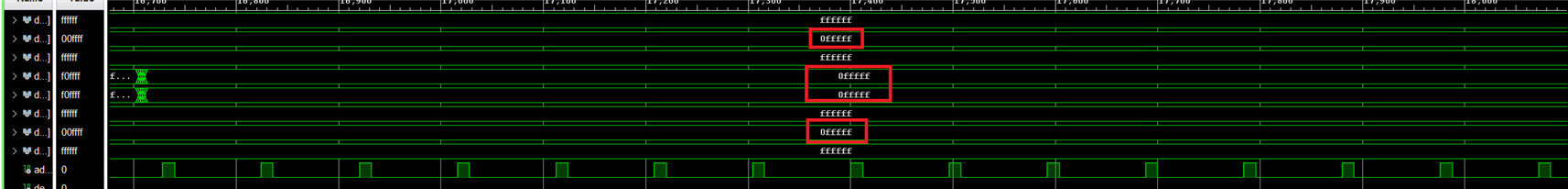
I am using the ADS9813 analog-to-digital converter. I operate the ads9813 in 2-lane SDR mode and I use the built-in test pattern with all one to fast bring-up the adc, and found that only channel 0 adn channel 7 with exactly all one pattern, which is 18'h3ffff. But the rest of channels pattern will looks like, 18'h03fff. I sampled the data at the rising edge of fclkout. I am wondering is there a fixed offset for a valid data frame between frame and the very first valid data bit?

Andy.Liu

  • Hi Andy,

    Thanks for your post. May I ask what kind of application you are using ADS9813 in?

    When you power on the device, please ensure you are:

    1. Providing a free running SMPL_CLK
    2. Completing the initialization sequence as listed in section 6.4.3 of the datasheet
    3. Providing a SMPL_SYNC pulse to align the output data index to FCLKOUT

    Then you may setup the test pattern. Could you share if the offset persists after these steps?

    Best regards,

    Samiha

  • Dear Samiha,

    I am using FPGA as the interface with ADS9813 EVM with FMC connection. I aim to program the ads9813 to operate in 2-lane SDR mode.

    I am sure that I follow the power-up procedure, and the I think the SPI initialization sequence I gave is correct. The following is the spi sequence I program the ads9813 registers for all one fixed test pattern.

                        4'd0: tmp = '{8'h04, 16'h000B};
                        4'd1: tmp = '{8'h03, 16'h0002};
                        4'd2: tmp = '{8'h92, 16'h0002};
                        4'd3: tmp = '{8'hC5, 16'h0604};
                        4'd4: tmp = '{8'hC1, 16'h0300};
                        4'd5: tmp = '{8'h13, 16'h0002};
                        4'd6: tmp = '{8'h14, 16'hFFFF};  // TP0_A[15:0] for pattern 24'hFFFFFF
                        4'd7: tmp = '{8'h15, 16'hFFFF};  // TP1_A[7:0]=0, TP0_A[23:16]=0xFF
                        4'd8: tmp = '{8'h16, 16'hFFFF};
                        4'd9: tmp = '{8'h18, 16'h0002};
                        4'd10: tmp = '{8'h19, 16'hFFFF};  // TP0_B[15:0]
                        4'd11: tmp = '{8'h1A, 16'hFFFF};  // TP0_B[23:16]
                        4'd12: tmp = '{8'h1B, 16'hFFFF};
    The issues are still there. I would like to share the screenshot. to show you the details.
    for some channels, there are 4-bit zero which should not be there
    Best regards
    Andy Liu
  • Hi Andy,

    Thanks for your patience as we were out of office for Thanksgiving holiday.

    Thanks for sharing the information. The register writes look correct. Did you pulse SMPL_SYNC signal once after the initialization sequence?

    I will check this on my side using the ADS9813EVM and get back to you.

    Best regards,

    Samiha

  • Hi Andy,

    Thanks for your patience as we were out of office for Thanksgiving holiday.

    Thanks for sharing the information. The register writes look correct. Did you pulse SMPL_SYNC signal once after the initialization sequence?

    I will check this on my side using the ADS9813EVM and get back to you.

    Best regards,

    Samiha

  • Dear Samiha,

    No problem.

    Yes, I did pulse SMPL_SYNC signal once after the initialization sequence. Looking forward to hearing from you soon.

    Best regards

    Andy Liu

  • Hi Andy,

    I tested this on an ADS9813EVM using 4-lane DDR and 4-lane SDR. Apart from setting the same 0xC1, I used the same register writes as you, and was able to see 0xFFFFFF outputs for all channels. The issue in your case may be that 2-lane SDR mode is not supported by this device. Could you please try 2-lane DDR or one of the supported modes?

  • Dear Samiha,

    Thanks for your reply. Actually, I have tried all the modes, 2-lane DDR, 4-lane DDR, and 4-lane SDR. Still could not see the all one pattern 0xffffff. 

    By the way, what is the available value of sampling clock frequency? Could it be any value between 3.9MHz ~ 8.1MHz from the datasheet? Or, only 4 and 8 MHz?

    Best regards,

    Andy Liu 

  • Hi Andy,

    How are you evaluating the ADC? Is it on your own board or are you using the ADS9813EVM? If using your own board, could you share the ADC schematic?

    Any SMPL_CLK value between 3.9MHz and 8.1MHz may be used. What clock value are you using?

    Could you also read back the register values in register 0x14, 0x15, 0x16 so we can verify that the registers are being written correctly? Are you seeing this issue on only one ADC?

    Best regards,

    Samiha

  • Dear Samiha,

    Thanks foy your reply.

    I am using the ADS9813EVM, and I have only one ADC. I've tried 4MHz and 8MHz under 4-lane DDR mode, but the results are still not all one. I will try to read back the register values later.

    Best regards,

    Andy Liu

  • Hi Andy,

    Good to know. If you are using ADS9813EVM, are you using it with the TSWDC155EVM controller card and the software GUI? If not, how are you powering the board? Better understanding your setup will help me isolate the source of the issue.

    Best regards,

    Samiha

  • Dear Samiha,

    I am not employing either of these two methods, TSWDC155EVM controller card and the software GUI. I am using a xilinx xczu15eg fpga with FMC to power the ADS9813EVM. I am using the example RTL codes( ADS98XX-FPGA-EXAMPLE-CODE V1.1.0) provided by TI for data capturing. I replace the IDDR primitive which is for Xilinx 7-series with IDDRE1 for ultrascale+ FPGA. It compiled successfully and for all one test pattern it passed. But when I switch to another test pattern by using SPI configuration, e.g. 24'h123456. The result doesn't match the test pattern even when I check every 24-bit in a frame. I still cannot figure it out.

    Best regards,

    Andy Liu


  • Hi Andy, 

    Thanks for sharing. If you had a TSWDC155EVM, we could confirm operation using the GUI. This sounds like it may be an issue with the deserializer code not parsing the output as expected. I am unfamiliar with the IDDRE1 primative so I cannot speak to it, but a quick google search shows me that the way the IDDR for Xilinx 7-Series and IDDRE1 may operate the clocks differently (looks like something about IDDRE1 needing true inverted clock). Just an idea, as my experience with FPGA code is limited, but I would try debugging there.

    Are you able to read the output of a few samples via a logic analyzer from the outputs of the ADC directly? That way we can confirm that the ADC is outputting the correct data. Reading back the test pattern registers, as I mentioned before, would also be a good debug step. 

    Best regards,

    Samiha

  • Dear Samiha,

    I've solve this problem using zynq-7000 series with TI-provided RTL example codes, which are compatible for Xilinx FPGA. I could see the waveform of 50mV sine wave at 1, 10, 100kHz. and also the ramp test pattern by switching the registers via SPI.

    Thanks a lot for your kindly help.

    Best wishes

    Andy Liu