This thread has been locked.

If you have a related question, please click the "Ask a related question" button in the top right corner. The newly created question will be automatically linked to this question.

AFE881H1: AFE881H1: Issues with 4-20mA Output Linearity and Current Floor at Low Setpoints

Part Number: AFE881H1
Other Parts Discussed in Thread: TLV431, OPA333

Description: I am working on a 4-20mA transmitter design using the AFE881H1. I have implemented the reference circuit exactly as shown in the datasheet with the recommended component values. However, I am experiencing issues with the output current accuracy and regulation.

Setup:

  • Loop Voltage: 24V DC

  • Load Resistance (Rload): 500 Ohm

  • Circuit: Standard reference design from the datasheet.

Observations:

  1. Non-Linearity at Low Current: When I set the input for a 15mA output (approx. 1.5V at the control point), the circuit works as expected. However, when I set it for 5mA (approx. 0.5V), the output current stays at 12.66mA.

  2. Current Floor: I cannot get any reading below 13mA; it seems to be hitting a floor.

  3. Supply Sensitivity: The output current changes when the 24V supply voltage is varied, indicating poor line regulation or an issue with the loop-powered regulation logic.

Questions regarding the Current Path: I am also having difficulty understanding the current flow logic described in the documentation:

  • The datasheet mentions that Q4 controls the current coming from the 24V source.

  • If the current (3mA to 25mA) flows through the 1k Ohm resistor located under Q4, the voltage drop would be between 3V and 25V.

  • With a 25V drop on a 24V system, Q4 would theoretically be cut off or unable to regulate.

Could you please clarify:

  1. What could be causing the output to saturate at 12.66mA instead of dropping to 4-5mA?

  2. How exactly is the current path distributed through Q4 and the sense/resistor network to avoid high voltage drops that would shut down the pass transistor?

  3. Are there specific grounding (COM vs. Loop-) considerations I might be overlooking that would cause the current to depend on the supply voltage?

Any guidance or troubleshooting steps would be greatly appreciated.
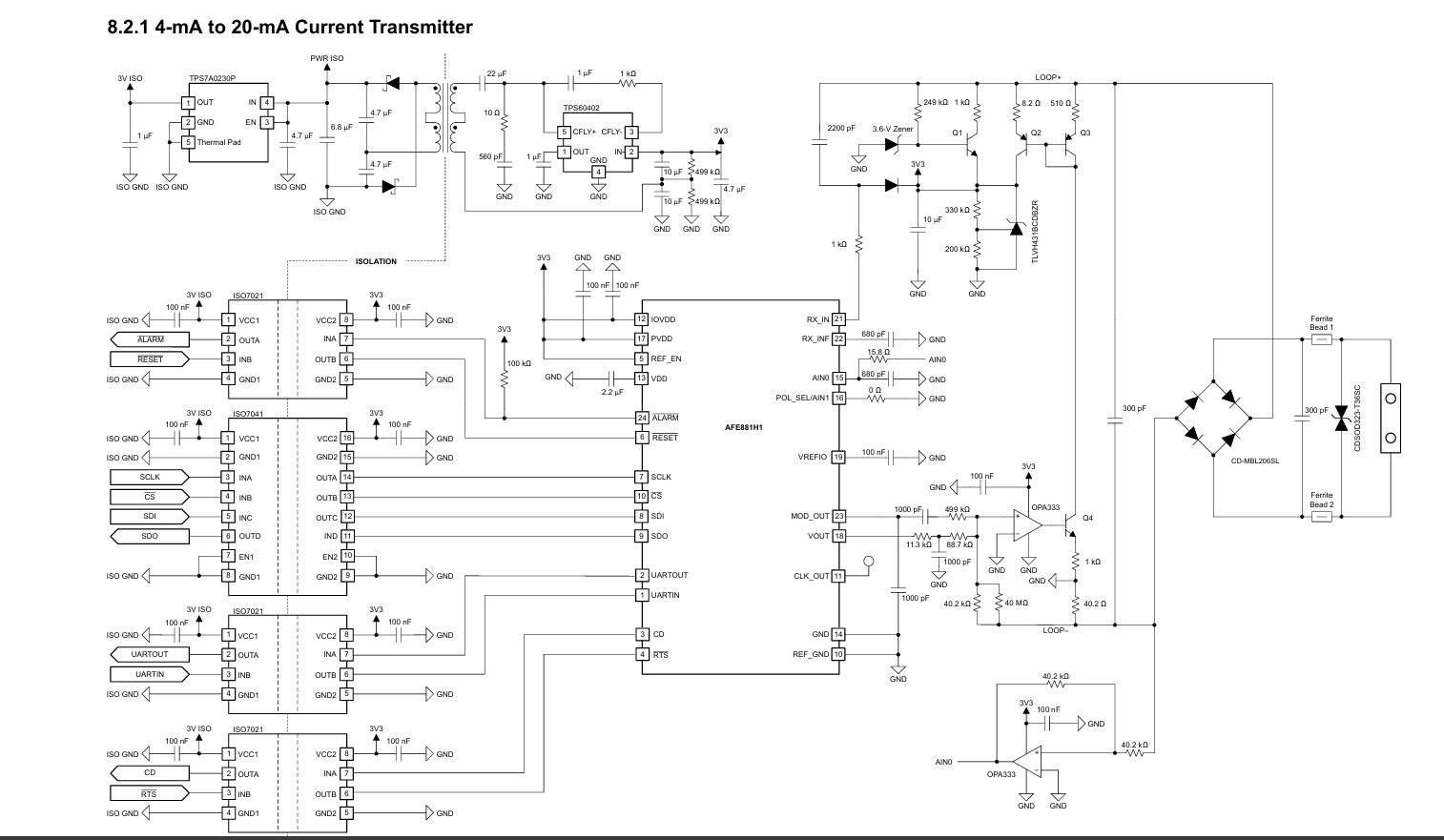


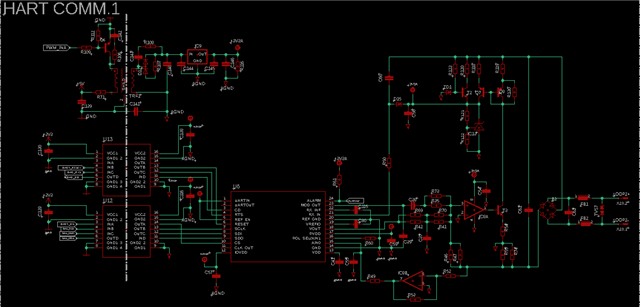
image.png

  • Hi Yusuf,

    I understand you said you implemented the circuit exactly as the one shown in the datasheet, but can you share your schematic so I can verify?

    Thank you,
    Lucas

  • Here are the component values used in the circuit, listed in order:

    • IC8 → MCP602-I/SN

    • T3 and T2 → NPN BC817-25/40

    • ZD1 → BZX84C3V6

    • Q7 and Q8 → PNP BC857C

    Regarding the resistors, only the values that differ are listed below. All other resistor values can be assumed to be the same as in the reference design:

    • R123 → 220 kΩ

    • R118 → 10 Ω

    • R119 → 680 Ω

    • R130 → Not connected

    With R130 not populated, the TLVH circuit is operating and I measure 3.3 V at the output.

    In addition to this, could you please explain where the current actually flows, whether it is in the microamp or milliamp range, and through which loop it returns? I may be overlooking the real fault mechanism.

    My concern is as follows:
    If mA-level current flows through R54 (1 kΩ), then T3 will not turn on. The op-amp output is 3.3 V — isn’t the current flowing from this output? If not, could you please clarify the actual current path?

    A step-by-step explanation of the current flow would be very helpful.


  • Hi Yusuf,

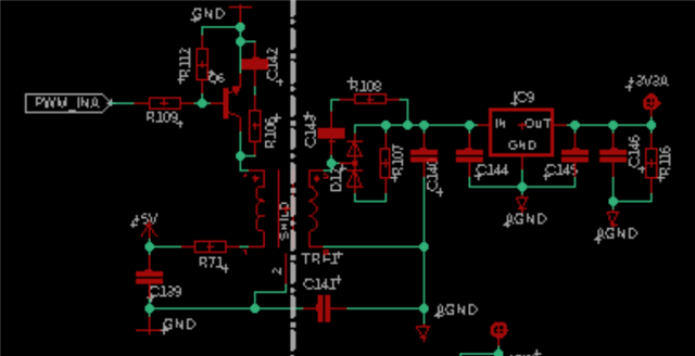
    You may be seeing the floor due to higher current consumption on your 3.3V net. If the current pull on the net goes past 3 mA, you will lose the ability to set the current output to below the current consumption value. This means you may be consuming ~13 mA from that net. Is it powering any other circuits not shown in the image?

    To doublecheck, is the 3.3V net by D15 connected to the circuit in the top-left corner? The resolution makes it hard to see the font.

    Thank you,
    Lucas

  • Hi Lucas,

    Before moving forward, I have a few questions regarding the current loops in this design.

    Could you please clarify or illustrate the specific paths where the current flows? Specifically, once the 3.3V rail is established via the startup circuitry, where does the current flow primarily?

    Furthermore, I would like to know the expected current magnitudes—are we looking at mA or µA ranges? Specifically, what is the calculated or typical current flowing through Q4 and the 1K resistor?

    Having this information will be very helpful, as I intend to verify the circuit’s operation through physical measurements.

    Thank you in advance for your support.

  • Yusuf,


    Short answer: Q4 to the emitter current of the 1kΩ resistor is on the order of about your loop current divided by 60. However, let me describe this in further detail below. I'll use the circuit shown in data sheet and refer to the transistors and resistor values that way.

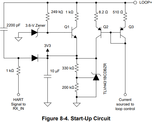
    The AFE881H1 data sheet starting at section 8.2.1.2.1 for the Start-Up Circuit (p96) describes how the currents flow in the circuit. Here's the basic start-up circuit shown in the data sheet:

    The Q1 and 1kΩ resistor are only used at start up. When power is first applied, the 249kΩ resistor sources some current to turn on the 3.6V zener. The base of Q1 is pulled up, which allows current to flow through the transistor. This turns on the TLV431 regulator and the voltage goes to 3.3V. As the regulator voltage increases to 3.3V, the VBE of Q1 drops (with 3.6V at the base and 3.3V at the emitter) and turns off the current.

    At the same time, the TLV431 regulator powers up the OPA333 and current starts to flow through Q2, Q3, and Q4. This feedback sets the loop current coming from the loop power.

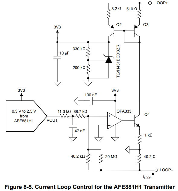
    After everything has stabilized, the current through Q1 is minimal. Q1 is only part of the startup and is shut down after the 3.3V regulator comes up. The current through Q2 and Q3 depend on the voltage at VOUT of the AFE881H1 DAC. In the above circuit, The DAC output current is VOUT/100kΩ. This current flows through the 40.2kΩ resistor. The OPA333 pulls up on the base of the transistor to pull loop current until the voltage across the 40.2Ω resistor matches the voltage across the 40.2kΩ resistor. This match give a 1000:1 current gain to set the loop current.

    Q2 and Q3 share the current load so that not all current goes through Q3 (and Q4). If the transistors matched, then the ratio of current for Q2 and Q3 would be 62:1. Even if the VBE of these transistors aren't exactly the same, there's a sizeable split between the Q2 and Q3 current. Regardless, the current through Q4 isn't basically the entire loop current.

    Because your loop current is working correctly as you get above 15mA, it means that the circuitry is pulling more current than expected. In the design, you'd want the circuit to work with a 3mA, and the loop's extra current is sunk by the TLV431 when the control is set to a higher current. If you're seeing 15mA, then you're pulling an extra 12-13mA or so through the existing circuitry.

    NOTE: We did notice there's an error in the diagram, which would require a change to the schematic. However, this should be easy to check. In the second OPA333 used to measure the LOOP- voltage, the opamp is drawn incorrectly and the feedback is attached to the positive input. You'll need to disconnect the resistor going to AIN0 and the resistor coming from LOOP-. Then you can attach a small wire to ground to the positive input of the op-amp. This should set the opamp to ground prevent extra supply current from being sunk through the loop.

    I'm not sure if this is the full problem. In the end, the OPA333 has a short circuit current limit of about 5mA, and it would take a little more current to reach the 15mA that you're seeing. Regardless, after tying down this second OPA333, I would expect the lower limit current to drop, and you can check to see if the current can be set below the 15mA you were seeing.


    Joseph Wu

  • Hi Joseph,

    Thank you for the clarification.

    I initially did not notice the AIN0 connection issue, as the AIN0 supply is currently not used in my setup. However, while reviewing the circuit in more detail, I identified another issue in the design.

    I am using a BZX84C3V6 zener diode in the startup circuitry. Due to the 220 kΩ series resistor, the zener is expected to operate in the microampere range, but this device is not stable at such low currents. When I tested the circuit, I observed that the zener continued to conduct current in an uncontrolled manner.

    To address this, I removed the startup circuit and modified the design so that the circuit is powered directly from the input through the regulator instead of relying on the startup network. With this change, the circuit now starts up correctly and operates in a stable manner.

    Regarding the AIN0 feedback / measurement circuit, after reviewing the schematic again, I see that the current configuration behaves partly like a comparator and partly like a Schmitt trigger, which is not the intended behavior. The correct implementation should be as shown below:

    Could you please review this configuration and confirm whether it is correct?

  • Apologies for the confusion — I realized that the schematic image I shared previously was incorrect.

    The correct circuit is the one shown below. In this configuration, –1 V is converted to +1 V using an inverting amplifier topology (gain = –1). This is intended to level-shift the LOOP– voltage into a range suitable for the ADC.

    Could you please confirm whether this approach and configuration are correct, or if you see any potential issues with this method?

  • Yusuf, 

    Yes, you are correct. The amplifier was set in inverting configuration to measure the LOOP- relation to ground. Because LOOP- is lower than ground, the inverting amplifier is used for the measurement at AIN0.

    Joseph Wu

  • The issue is resolved now. Thank you for your support and guidance.