Part Number: ADC3563
Other Parts Discussed in Thread: THS4541, LM7705
Hi there,
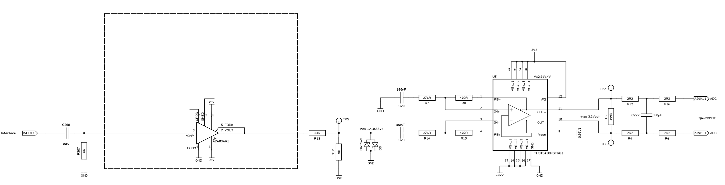
We are designing an ADC3563 based IF sampling circuit and we are at a point where we are discussing protection methods for the AINP/M pins.
Since the absolute maximum ratings for those pins in the datasheet specify a range of -0.3V to MIN(2.1, AVDD+0.3)V, and our AVDD is 1.8V, the effective maximum rating for our case is -0.3V to 2.1V.
The analog front end driving the ADC3563 contains a single-ended to differential stage using a THS4541 which is supplied with -0.23V (via LM7705) and 3.3V.
Under normal operation, the ADC3563 should never see voltages exceeding its ratings. However, since the positive rail of the THS4541 is 3.3V, there is a risk that the amplifier output could drive the ADC inputs above 2.1V (e.g. during startup transients or faults), which would destroy the ADC.
What is the best way to protect the AINP/M inputs in this specific design?
We considered inserting a BAT54S Schottky diode pair between the initial amplifier stage and the THS4541 input to limit the signal before the final amplification. However, I have concerns about this approach:
-
An error in the final amplification stage (e.g. wrong gain resistor placement during production) could still result in the ADC being destroyed.
-
I would prefer to avoid the non-linear capacitance of the BAT54S in the signal path.
I have read about TVS diodes and using current limiting series resistors, but I would appreciate advice from experienced engineers on how to proceed in this specific case to ensure the ADC is safe without compromising AC performance.
Thanks in advance!
Maik