


Part Number: DAC39RF12EVM
Other Parts Discussed in Thread: TSW14J59EVM
Dear TI team,
I would like some help to bring up the JESD link running between DAC39RF12EVM and TI JESD IP.
I already tried to read up on existing related posts such as this DAC39RF10EVM: Unable to get JESD link up with TI JESD IP and ZCU102 example design - Data converters forum - Data converters - TI E2E support forums . However, I did not find any solution. Therefore, any help would be appreciated.
Description: I used the reference design provided for ZCU102 and TI JESD IP and modified it for ZCU111. The reference design internally has a 64point sine wave which I am using to test the DAC in JESD mode. I configure the reference design to use in "TX only" mode.
I am providing a 4GHz sampling clock to the EVM (instead of 10.24 GHz due to equipment capability) and 125MHz reference clock. ZCU111 is connected via FMC connector.
I am configuring the DAC for JMODE1, real data, 1 channel, 16b, 8 lanes, 8b10b encoding in subclass1 operation. SYSREF K factor = 32. I have also verified that LMFS parameters match (8-1-2-8). I use the DAC EVM GUI to configure the LMK, DAC and the clocks.
After configuring the DAC via the EVM GUI and programming the FPGA, I am able to get the SERDES PLLs locked, SYSREF align statuses are also green on the GUI. I also noticed that DAC SYNCN (out from the DAC) goes high on the ILA on the FPGA side. However, JESD link and 8b/10b SYNC statuses are still "red" and I am unable to get the link working.
I would appreciate any useful help or directions to help me debug the JESD link. 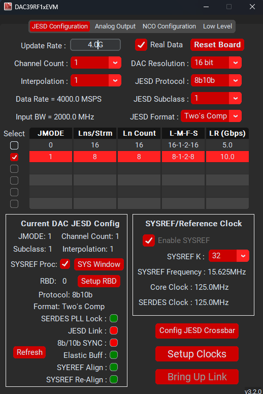
Also, I would like to request, if possible, the FPGA reference design used on TSW14J59EVM with DAC39RF12EVM to test the DAC in JESD mode. This could also be a useful starting point. Regardless, appreciate any useful hints/directions for debugging further. Many thanks.
