Part Number: ADC3662EVM
Other Parts Discussed in Thread: ADC3662
Hello Experts,
i have FPGA mother board from TrenzElectronic TEBF0818 assembled with TE813 FPGA core board connected to TI ADC3662EVM module rev. E (1-wire 10MSPS mode, all LVDS terminated by 100ohm inside FPGA I/O cell)modified per following steps:
-
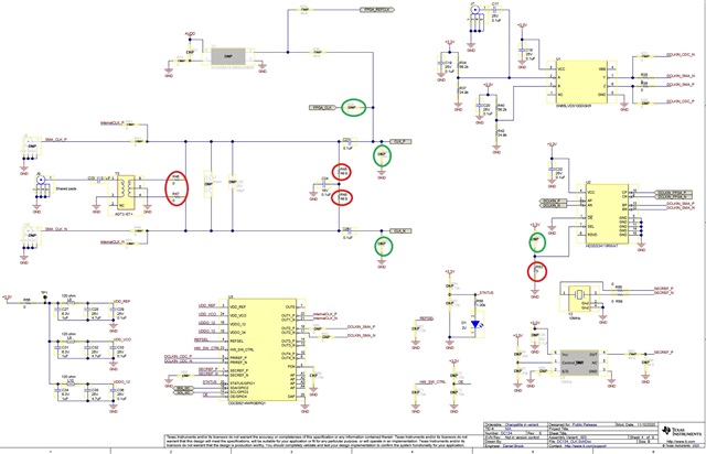
Unmount R46 (0 Ohms) and R47 (0 Ohms). This will disconnect differential clock signal coming from J9 from CLK_P and CLK_N.
-
Mount R39 (0 Ohms). This will connect FPGA_CLK with CLK_P
-
Unmount R45 (49.9 Ohms) and R48 (49.9 Ohms). This will remove differential clock termination
-
Mount R44 (49.9 Ohms). FPGA_CLK single ended clock termination
-
Mount R52 (0 Ohms). FPGA_CLK single ended clock termination
-
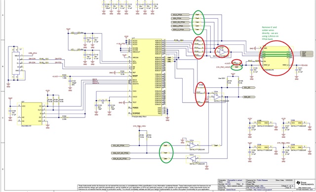
Unmount R150 (0 Ohms) and mount R151 (0 Ohms). This is to be consistent with FPGA IO voltage
-
Unmount R139 (0 Ohms) and mount R133 (0 Ohms). This will disconnect SCLK signal coming from FTDI chip and will connect SCLK_FPGA signal coming from FPGA.
-
Unmount R140 (0 Ohms) and mount R134 (0 Ohms). This will disconnect SEN signal coming from FTDI chip and will connect SEN_FPGA signal coming from FPGA.
-
Unmount R141 (0 Ohms) and mount R135 (0 Ohms). This will disconnect SDIO_OE signal coming from FTDI chip and will connect SDIO_OE_FPGA signal coming from FPGA.
-
Unmount R142 (0 Ohms) and mount R136 (0 Ohms). This will disconnect SDIO_I signal coming from FTDI chip and will connect SDIO_I_FPGA signal coming from FPGA.
-
Unmount R144 (0 Ohms) and mount R137 (0 Ohms). This will disconnect SDIO_O signal coming from FTDI chip and will connect SDIO_O_FPGA signal coming from FPGA.
-
Unmount R156 (0 Ohms), mount R165 (0 Ohms), mount R166 (0 Ohms). This will disconnect SCL_I2C signal coming from FTDI chip and will connect SCL_I2C_FPGA signal coming from FPGA.
-
Unmount R157 (0 Ohms) and mount R167 (0 Ohms). This will disconnect SDA_OUT_I2C signal coming from FTDI chip and will connect SDA_OUT_I2C_FPGA signal coming from FPGA.
-
Unmount R161 (0 Ohms) and mount R168 (0 Ohms). This will disconnect SDA_IN_I2C signal coming from FTDI chip and will connect SDA_IN_I2C_FPGA signal coming from FPGA.
-
Unmount R53 (0 Ohms) and mount R50 (0 Ohms). This will connect DCLKIN differential signal to DCLKIN_FPGA differential signal and not to DCLKIN_SMA differential signal.
-
Remove SMA connectors J4 & J6. These connectors are in conflict with SFP cage in Zynq Ultrascale+ evaluation board. They provide differential analog interface for input signal of ADC channel B, which will not be used during testing.
-
Unmount component U18 (LSF0204RUTR) and connect its pins as described below:
-
pin 7 (B4) -> pin 5 (A4)
-
pin 8 (B4) -> pin 4 (A4)
-
pin 9 (B4) -> pin 3 (A4)
-
Unmount component U19A (SN74LVC1G125DCKT)
This is necessary to comunicate with ADC3662 from FPGA right? But i am not able to read non zero default value from the register 0x20, 0x21 and 0x22. I am using custom serial FPGA driver to communicate with it. I am able to write registers from 0x00, 0x07,...0x34 and after that i read all correct values from the registers. So i think the serial driver wotks correctly. But after reset i am not able to read default non zero values from 0x20, 0x21 and 0x22 - always read zeros.
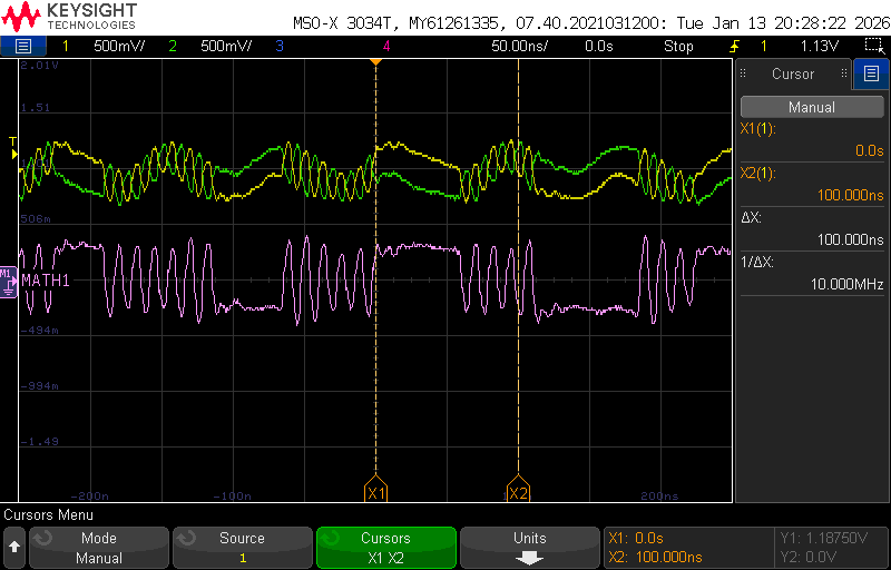
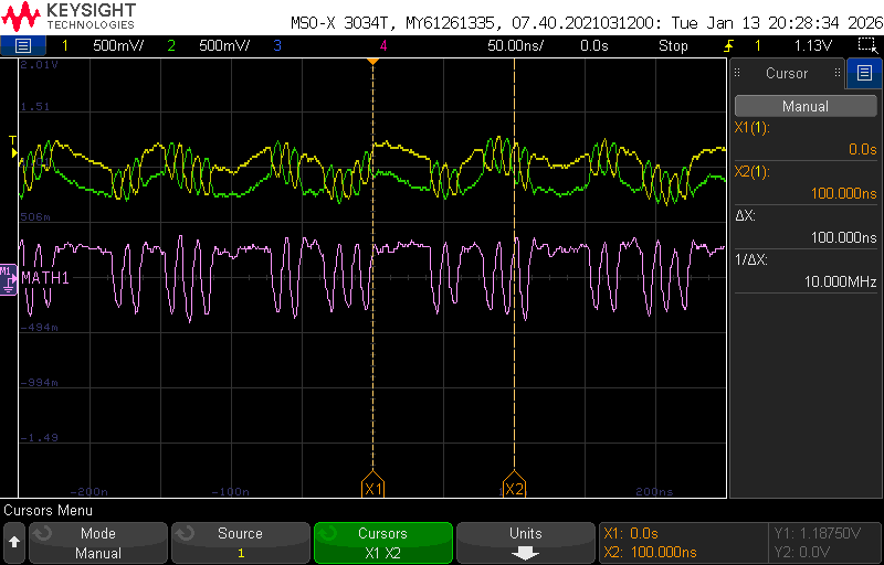
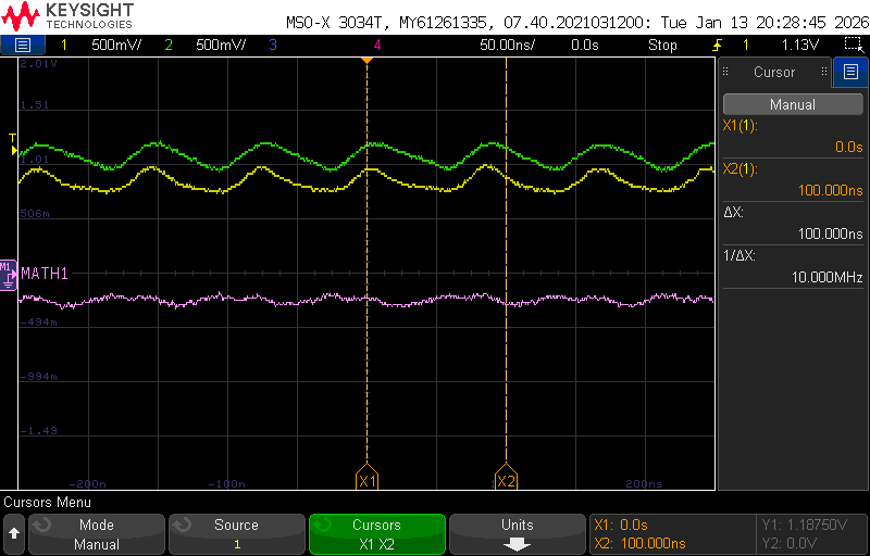
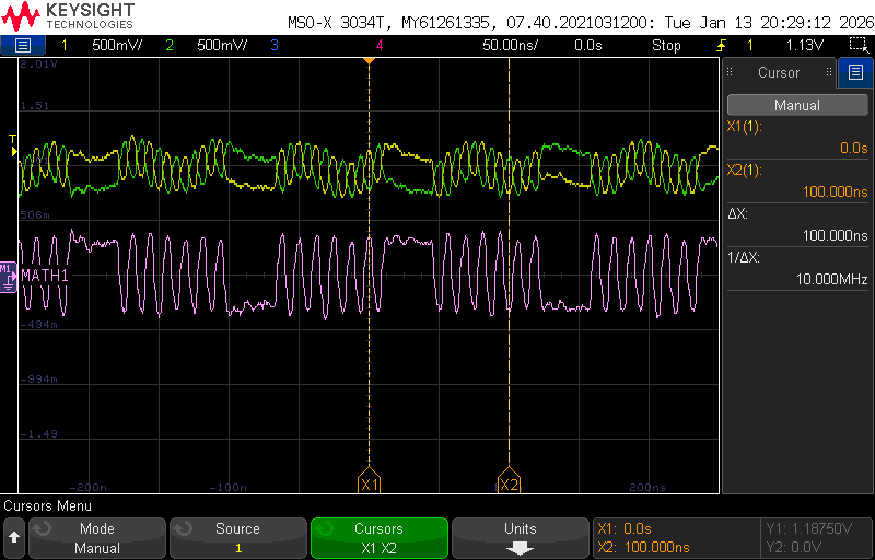
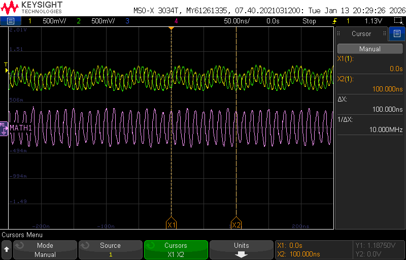
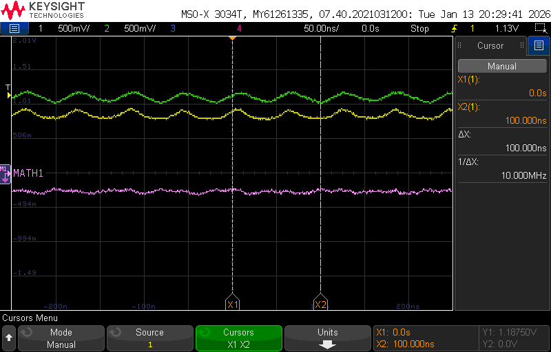
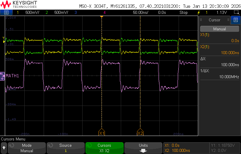
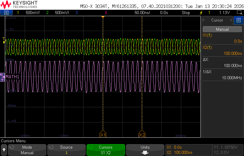
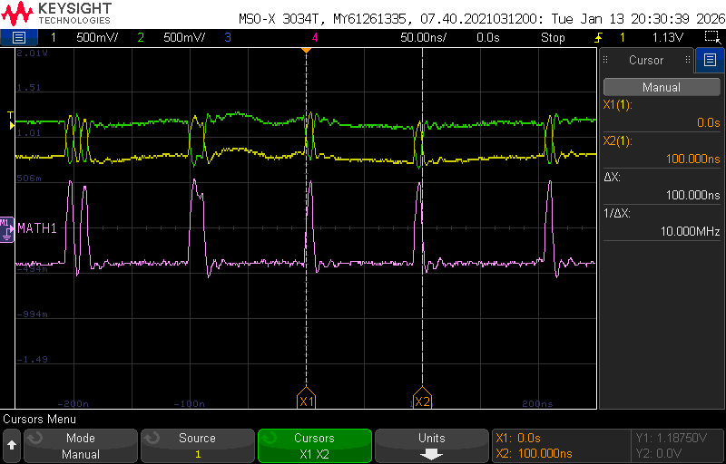
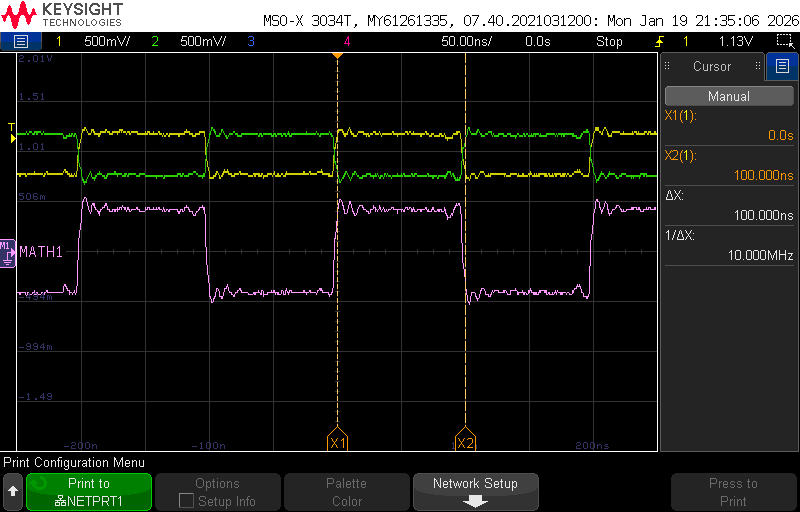
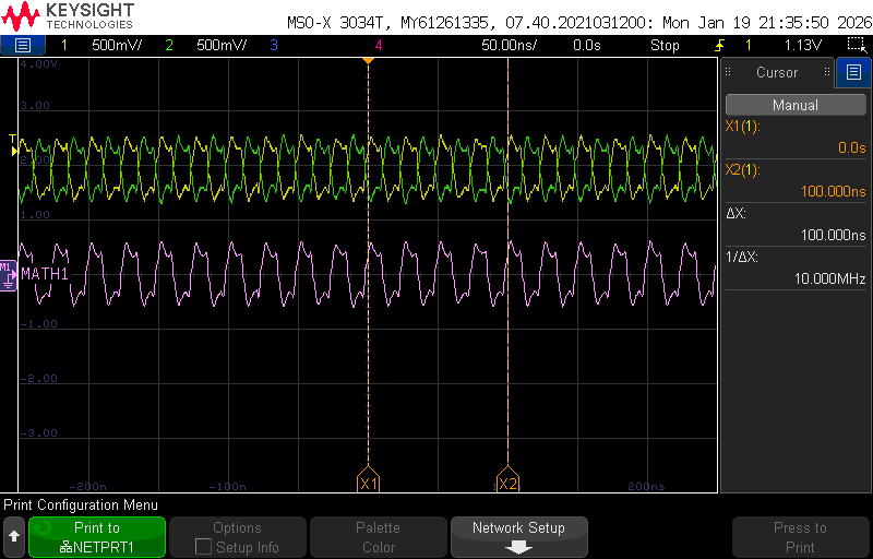
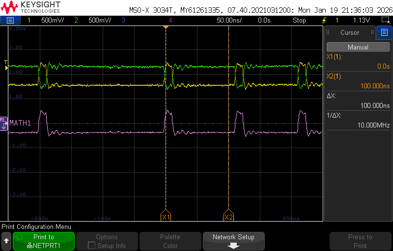
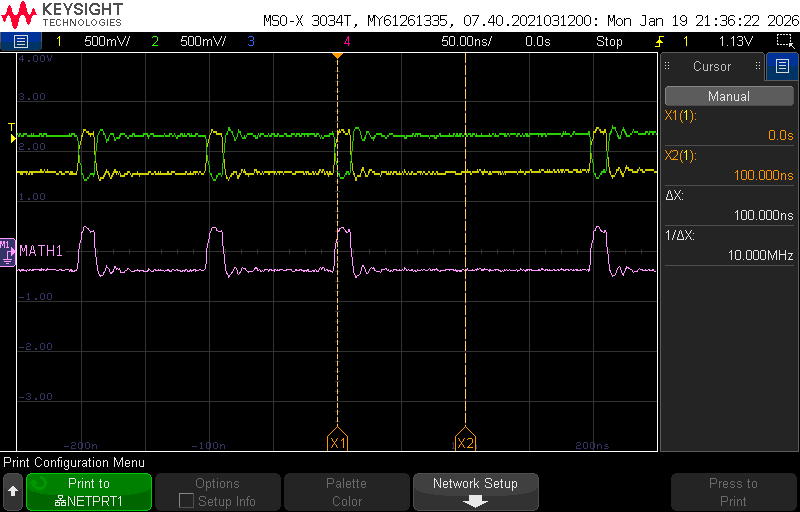
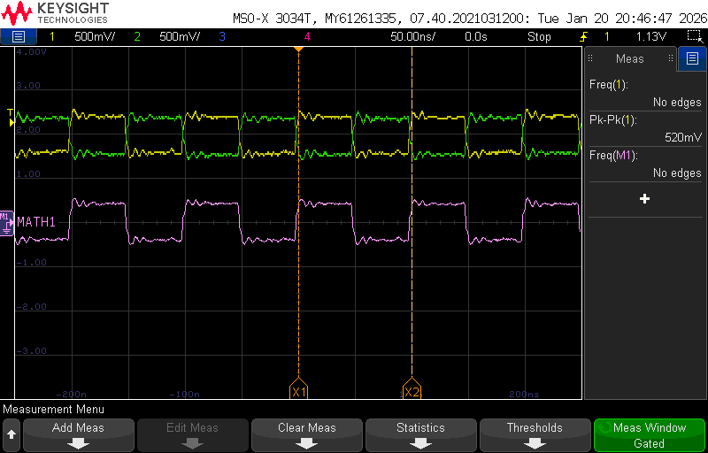
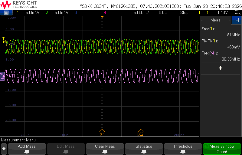
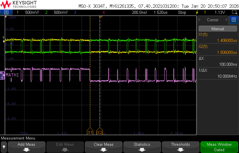
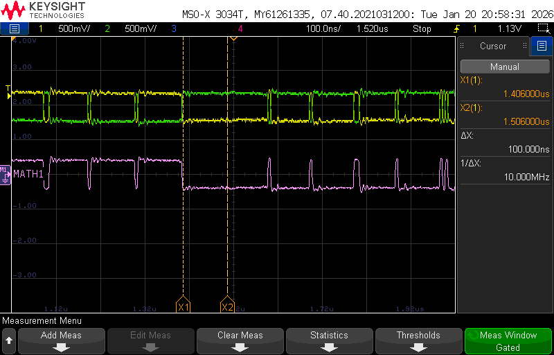
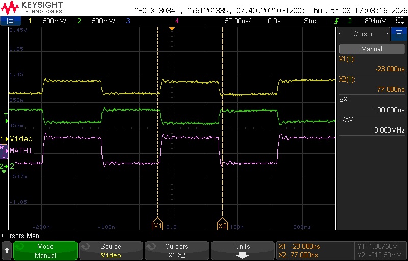
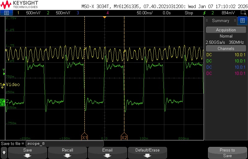
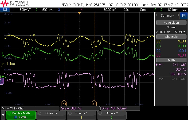
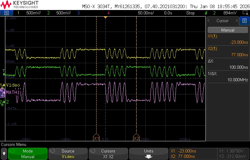
Additionaly i am generating DCLKIN = 80MHz as LVDS 1,8V and CLK = 10MHz 1,8V single ended. Both clock are generated from one PLL = phase aligned. But sometimes i observe returned DCLK from FPGA with missing periods and FCLK with oscillation before and after expected rise/fall edges. I saw only once FCLK without these artefacts but after power down and power up it goes into issue again.
I saw this only once (DCLK=100MHz, CLK=10MHz) - after power down->power up i saw again something similar like next printscreen with DCLK=100MHz, CLK=10MHz.
Also i see, that with the same setup of HW and serial configuration the waveforms changes after power down and power up.
I tried it without any initialisation to 1-wire 16bit and with the initialisation but the similar result. The waveforms still seems bad.
This is setup i tried:
Write_ADC_register(0x00, 0x01);
    Delay(100000000);


    Read_ADC_register(0x20);
    Read_ADC_register(0x21);
    Read_ADC_register(0x22);

    Write_ADC_register(0x07, 0x6C);
    Write_ADC_register(0x13, 0x01); // E-Fuse load
    Delay(100000000);
    Write_ADC_register(0x13, 0x00);
    Write_ADC_register(0x19, 0x00); // FCLK config

    Write_ADC_register(0x1B, 0x88); // Set resolution


    Write_ADC_register(0x20, 0x00); // FCLK pattern
    Write_ADC_register(0x21, 0xF0); // FCLK pattern
    Write_ADC_register(0x22, 0x0F); // FCLK pattern


    //Write_ADC_register(0x08, 0x00);
    //Write_ADC_register(0x09, 0x0B); // Disable DA1/DB0/DB1
    //Write_ADC_register(0x09, 0x00); // Enable all Data lanes
    //Write_ADC_register(0x09, 0x30); // Disable DCLK, FCLK
    //Write_ADC_register(0x19, 0x10);
    Write_ADC_register(0x24, 0x00);
    Write_ADC_register(0x25, 0x00);
    Write_ADC_register(0x08, 0x02); // Disable B channel
    Write_ADC_register(0x09, 0x0B); // Disable DA1, DB0, DB1
Yellow -> FCLK_P, green FCLK_N, pink -> diff FCLK_P-FCLK_N
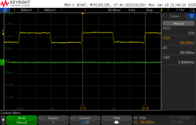
Yellow -> DCLK_P=80MHz, green CLK(single ended)=10MHz
Weird FCLK_P/N behaviour when DCLK=80MHz, CLK=10MHz
Regards,
Petr Burda