Part Number: ADS9229
Dear TI Team,
We are now able to collect statistical information on the precision of our design based on ADS9229. It seems that the offset due to the ADC is dominant, as opposed to the rest of the analog chain. In that context, we have the following questions:
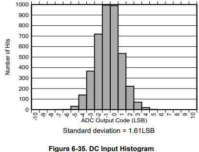
- Do you have any statistical information on the offset distribution of the ADC itself? The datasheet mentions +-10LSB, which seems consistent with our worst-case measurements (hence ±2sigma), but we'd like to make sure that our analysis is correct in the first place.
- Is there really no offset compensation register hidden somewhere?
- There is apparently a "gain error compensation" mechanism integrated inside the chip and taking place during initialization (which we're using). We, however, haven't found any information on how this works exactly, and if there are any potential links to offset compensation as well. Any comments or recommendations? We have a system-level initialization sequence anyway...
As of now, we're implementing calibration inside the related FPGA driver, but we'd rather leverage any existing mechanism, if any.
Looking forward to your feedback,
WBR,