Part Number: ADC12DJ2700
Other Parts Discussed in Thread: AFE7950
Hi TI ,
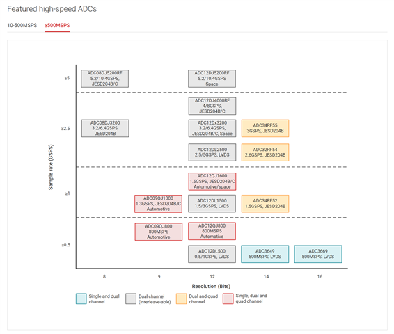
I am currently working on a system design that uses the ADC12DJ2700 high-speed ADC in combination with a Xilinx Kintex UltraScale FPGA (XCKU085-1FLVA1517I). I would appreciate your technical guidance on the suitability of this device combination and recommended design practices.
The key system-level ADC requirements are as follows:
-
Input Frequency Range: 0.8 GHz to 6 GHz
-
Number of RF Inputs: 4
-
Required Dynamic Range: 60 dB
-
Signal Types: Continuous Wave (CW) and pulsed signals
-
Instantaneous Bandwidth: 1 GHz
Based on these requirements, I would like your advice on the following points:
-
Device Suitability
Is the ADC12DJ2700 an appropriate choice for meeting the above performance requirements? -
FPGA Compatibility
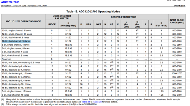
Is the Kintex UltraScale XCKU085-1FLVA1517I a recommended FPGA for interfacing with the ADC12DJ2700 (including JESD204B/C bandwidth, lane count, and processing margin)? -
Reference Designs and Documentation
While reference designs are available for devices such as the AFE7950, we have not been able to locate equivalent reference designs for the ADC12DJ2700.
Could you please share any existing reference designs, evaluation platforms, application notes, or relevant documentation for this device? -
Device Initialization and Configuration
What is the recommended approach for ADC12DJ2700 device initialization and configuration when used with a custom FPGA platform based on the Kintex UltraScale family?
Please let us know of any additional application notes, design guidelines, or best practices that would be helpful for implementing this ADC–FPGA combination.
The same case I have already raised through the TI customer support center and the case number is CS3192547.
Thank you for your support. I look forward to your guidance.
Regards,
Sivakumar S