This thread has been locked.

If you have a related question, please click the "Ask a related question" button in the top right corner. The newly created question will be automatically linked to this question.

DAC7716: Reasons for malfunctions

Part Number: DAC7716

Hi  Team,


I have three questions about the DAC7716.

■ Operating conditions
- AVDD = +15 V, AVSS = −15 V
- DVDD = 5 V, IOVDD = 5 V
- VREF = 5 V
- RST = 5 V (reset deasserted during power-up)
- UNI/BIP-A = UNI/BIP-B = 5 V
- LDAC = 0 V
- VOUT-x = RFB1-x = RFB2-x shorted (voltage output mode)
- Hardware gain = ×4
- No series resistor on VOUT

Below are the questions we would like to confirm:

1) RST high during power-up  
Is there any risk of latch-up or device damage if the RST pin is already high (reset released) during power-up?

2) No series resistor on VOUT  
If the DAC output is directly connected to the load (no series resistor), is there any risk of overcurrent damage, for example in the case of a short to GND or a heavy load?

3) Gain mismatch  
If the hardware gain setting (e.g., ×2) and the command register gain setting (e.g., ×4) are different:  
- Could this cause device damage?  
- How is the actual output voltage scale determined in this case?


Best Regards,

Shota

  • Hi Shota,

    1) Leaving RST high during power up should not create any latching issues. As long as you follow the recommended sequence order on page 22 of the datasheet, the device should initialize as expected.

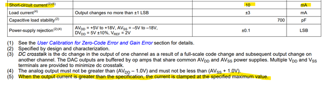
    2) The output current of each channel is clamped when the load exceeds its max capability defined in the specification table. This process should not result in device damage assuming there were no absolute maximum specifications violated during the event.

    3) Let me double check this one and get back to you. I wouldn't expect this to damage anything but I need to verify the output behavior when the hardware doesn't match the gain register setting. When the device is reset, the gain bits are returned to their default value of 1'b so if you have the hardware configured for a gain of 2 this will be a mismatched case. I doubt the device is designed in such a way to create damage in such a scenario since this could easily happen during normal operation.

    Regards,

    James

  • Hi, James-san,

    Thank you for your reply. I look forward to your continued support regarding question 3. I apologize for asking an additional question, but could you please confirm the following? I understand the sequence. 

    You said that the REF pin is powered up after AVDD and AVSS to avoid activating the ESD protection circuit, but as long as AVDD is at a higher voltage than REF, there's no problem, right? 

    In other words, if REF is stable at 5V, but AVDD hasn't yet reached 15V and is in the middle of powering up, is there a possibility that the internal circuitry is not operating and malfunctions may occur?

    Also, what voltages are required on AVDD and AVSS for the device to operate? Will the device start operating at ±4.75V, the minimum value listed in the datasheet, even during ramp-up?

    Best Regards,

    Shota

  • Hi Shota-san,

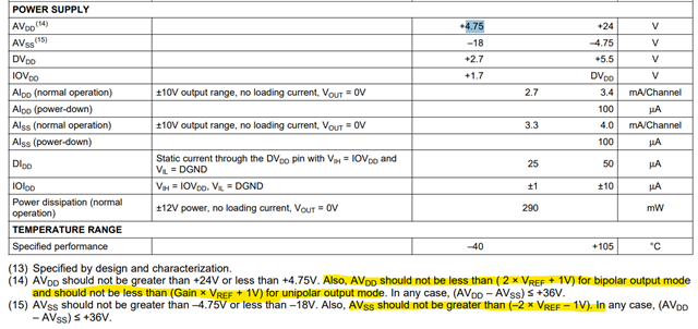
    Yes, as long as the AVDD is above REF, the ESD should not engage. Specifically I would make sure you follow these specification footnotes found in the datasheet regarding the AVDD / AVSS levels relative to VREF:

    If REF is already at 5V before AVDD has even started then you could be running current through the ESD circuitry which is inadvisable.

    The device should be ready once AVDD and AVSS reach their minimum operating thresholds but keep in mind that you will need to wait for AVDD and AVSS depending on your DAC output needs. If you're planning to use +/-10V at the DAC output then +4.75V on AVDD won't be enough and you will need to wait for the supply rails to reach your desired levels.

    Regarding question 3 from your previous post, the GAIN bit controls some switches that connect the feedback resistors to the input of the op amp in the R-2R structure. The GAIN bit setting needs to match the hardware connections so that the R-2R ladder switch resistance is accounted for in the feedback resistance from what I understand.

    Essentially, if the GAIN bit does not match the hardware setting, one of the feedback resistors will be open circuit from inside the IC package and you will end up with the higher gain setting of 4x. This mismatch would not cause damage, just an incorrect gain setting from what you might expect. If you are already using a gain of 2x on the hardware side, I don't think the mismatch matters since one of the feedback resistors will be disconnected by the external pin connection anyway.

    The red marks in the image below show where these switches would be for context:

    Regards,

    James

  • Hi James-san,

    I apologize for the additional question, but my customer is operating the device under the following conditions that I initially provided. They are experiencing issues where the device heats up to around 90°C, or, even when it does not heat up, it fails to deliver the expected output according to the settings.
    Are there any possible causes other than the sequence that we should consider?


    Below are the conditions:

    - AVDD = +15 V, AVSS = −15 V
    - DVDD = 5 V, IOVDD = 5 V
    - VREF = 5 V
    - RST = 5 V (reset deasserted during power-up)
    - UNI/BIP-A = UNI/BIP-B = 5 V
    - LDAC = 0 V
    - VOUT-x = RFB1-x = RFB2-x shorted (voltage output mode)
    - Hardware gain = ×4
    - No series resistor on VOUT

    Best Regards,

    Shota

  • Hi Shota-san,

    Can you share your schematic and layout so I can take a look? I can set up a private space to share these if you would prefer.

    Also, can you describe your DAC settings in more detail?

    • Do all the DAC channels show the same incorrect output behavior?
    • What is the input data setting for DAC-0 for example? How does this compare to the output after you attempt to write the new input data?
    • Does changing the gain bit from x4 -> x2 and x2 -> x4 result in an output change?
    • Is the output voltage a multiple of the input code or is the output error a random offset value?
      • If the VOUT error is small, this might be fixable with Zero or Gain error adjustment settings.
      • Is the output voltage stuck at 0V even after attempting to write a new input code?

    • Are you able to see your input current for the analog supplies? High temperatures would suggest excessive current flow somewhere which leads to increased power dissipation.
      • If you are violating the power sequence recommendations, this could be flowing unexpected current through the ESD cell from a REF pin. If you can share the power sequence waveforms from a scope, or current information from your power source it might reveal the issue. 
      • Any risk of the thermal pad not having full connection to the board?
      • What is the ambient temperature around the IC?

    For a gain setting of x4, you should have RFB1-x connected to VOUT-x and RFB2-x should be floating. I would match this hardware setting with the gain bit setting to be in-line with the datasheet recommendation if possible.

    Regards,

    James

  • Hi James-san,

    Thank you for your response.
    I will share the waveforms via private message. Please wait a moment.
    I would like to confirm the following question again:

    When RFB1-x and RFB2-x are connected to VOUT-x and the corresponding GAIN bit in the command register is set to '1', is it correct to understand that if the hardware is set to ×2 and the command register is set to ×4, the resulting gain is ×4?
    My customer is getting the following output with the following settings. In other words, the gain is 2. Why is this? Could you please explain?


    INPUT_CODE: 0, Output Voltage: 0V
    INPUT_CODE: 1024, Output Voltage: 2.50V
    INPUT_CODE: 2048, Output Voltage: 5.06V
    INPUT_CODE: 4095, Output Voltage: 10.1V

    Best Regards,

    Shota

  • Hi Shota-san,

    My assumption before was that the Gain bit was opening and closing some switches connected to the internal resistors on the RFB lines, but if the Gain bit is not changing the output gain when you have both RFB1-x and RFB2-x shorted to VOUT-x that would suggest that the hardware setting takes priority over the Gain bit setting somehow.

    If the Gain bit is not allowing you to achieve x4 gain then the only other option is to change the RFB connection as well.

    Just to be clear, you see no change in the output if you toggle the Gain bit in your situation?

    Regards,

    James

  • Hi James-san,

    I changed the gain setting to Gain = 2 and Gain = 4 in the command register, but the output did not change in either case. Does this mean that the hardware configuration takes priority?
    Also, is it possible that the command register is not being communicated correctly?

    Even when I set DB5 to DB2 to 1 as shown below, the readback value remains 0.
    Is this caused by an incorrect readback of the command register?
    Best Regards,
    Shota
  • Hi Shota-san,

    Your question about incorrect readback is a bit confusing. It looks to me like your GAIN = 4 setting was received correctly. On the right side of the image, the readback of the command register is showing DB5:DB2 = 1111'b. I don't see a write command followed by an incorrect read anywhere.

    I do see that your voltage appears to remain the same which suggests that the hardware determines the gain rather than the bit setting.

    Test the hardware change as soon as possible. I recommend changing the hardware to achieve a gain of 4 and then try the same test where you change the Gain bit to see if it has any affect on the output.

    Regards,

    James

  • Hi James-san,

    Thank you for your response.

    My customer is currently checking on this.

    I have one more question.

    Why does the hardware setting take precedence even though there is a switch inside?

    Best Regards,

    Shota

  • Hi Shota-san,

    I'll run this question by our design team again. The original explanation was the switches but since the hardware seems to take priority there must be some other mechanic at play.

    Regards,

    James