This thread has been locked.

If you have a related question, please click the "Ask a related question" button in the top right corner. The newly created question will be automatically linked to this question.

ADS8686S: Data is getting delayed by 1 channel

Part Number: ADS8686S
Other Parts Discussed in Thread: ADS9324

Hello, 
   We are using TMS570LC43xx and ADS8686S on SPI, 1 wire software configuration.
We are getting correct data but it is shifted to the next channel. 
For eg. All channels A0-7, and B0-7 channels are connected to 0.59V except Channel A2 is connected to 0 or ground but in the data we are seeing Channel 3 is getting data as 0. which is incorrect.
I have attached output and code.
 Please help us resolve this issue.

Thanks!!

        Reading ADC 1
Value of ADC-A CH0 is 0x0F2B and Raw Value is 0.593V
Value of ADC-B CH0 is 0x0F2B and Raw Value is 0.593V
Value of ADC-A CH1 is 0x0F2D and Raw Value is 0.593V
Value of ADC-B CH1 is 0x0F2D and Raw Value is 0.593V
Value of ADC-A CH2 is 0x0EFA and Raw Value is 0.585V
Value of ADC-B CH2 is 0x0EFA and Raw Value is 0.585V
Value of ADC-A CH3 is 0x0001 and Raw Value is 0.000V
Value of ADC-B CH3 is 0x0001 and Raw Value is 0.000V
Value of ADC-A CH4 is 0x0E14 and Raw Value is 0.550V
Value of ADC-B CH4 is 0x0E14 and Raw Value is 0.550V
Value of ADC-A CH5 is 0x0F2C and Raw Value is 0.593V
Value of ADC-B CH5 is 0x0F2C and Raw Value is 0.593V
Value of ADC-A CH6 is 0x0F2D and Raw Value is 0.593V
Value of ADC-B CH6 is 0x0F2D and Raw Value is 0.593V
Value of ADC-A CH7 is 0x0F2C and Raw Value is 0.593V
Value of ADC-B CH7 is 0x0F2C and Raw Value is 0.593V
Value of ADC-A CH8 is 0x0F2A and Raw Value is 0.592V
Value of ADC-B CH8 is 0x0F2A and Raw Value is 0.592V
Value of ADC-A CH9 is 0x67BE and Raw Value is 4.052V
Value of ADC-B CH9 is 0x67BE and Raw Value is 4.052V

void readADC(void){
    char testString[100] = {0};

    uint8_t index = 0x00; /// To Read All Channels

    uint16_t cmd = 0x0000; /// To pack the Command
    uint16_t cmdDummy = 0x0000; /// Dummy data to send

    uint16_t dataBuff[10] = {0}; /// Buffer for Read

    sprintf(testString, "\tReading ADC 1\n\r");
    sciDisplayText(sciREG3, testString);

    cmd = 0x8400; /// Config Register
    adcSpiCfg.CSNR = CS_ADC1;
    extAdc_WriteReg(cmd, dataBuff);

    cmd = 0x88AA; /// Range Select CH A1
    adcSpiCfg.CSNR = CS_ADC1;
    extAdc_WriteReg(cmd, dataBuff);

    cmd = 0x8AAA; /// Range Select CH A2
    adcSpiCfg.CSNR = CS_ADC1;
    extAdc_WriteReg(cmd, dataBuff);

    cmd = 0x8CAA; /// Range Select CH B1
    adcSpiCfg.CSNR = CS_ADC1;
    extAdc_WriteReg(cmd, dataBuff);

    cmd = 0x8EAA; /// Range Select CH B2
    adcSpiCfg.CSNR = CS_ADC1;
    extAdc_WriteReg(cmd, dataBuff);

    cmd = 0x8600; /// Select CH0
    for(index = 0; index < 10; index++){ /// Loop to increment Channel A and B by 1

//        extAdc_WriteReg(cmd, dataBuff); /// Write channel number to get ADC Conversion Value
 
        gioSetBit(spiPORT1, ADC1_CONV_PIN, 1); /// Start conversion
        while(gioGetBit(spiPORT1, ADC1_BUSY_PIN) != 1);
        gioSetBit(spiPORT1, ADC1_CONV_PIN, 0);
        while(gioGetBit(spiPORT1, ADC1_BUSY_PIN) != 0);


        adcSpiCfg.CS_HOLD = FALSE;
        adcSpiCfg.CSNR = CS_ADC1;
        spiTransmitAndReceiveData(ADC_SPI, &adcSpiCfg, 2, &cmdDummy, dataBuff); /// Read ADC value

        sprintf(testString, "Value of ADC-A CH%d is 0x%04X and Raw Value is %0.3fV\r\n", index, dataBuff[0], ((((float)dataBuff[0])/65535.0f)*10.0f));
        sciDisplayText(sciREG3, testString);

        sprintf(testString, "Value of ADC-B CH%d is 0x%04X and Raw Value is %0.3fV\r\n", index, dataBuff[1], ((((float)dataBuff[1])/65535.0f)*10.0f));
        sciDisplayText(sciREG3, testString);

        cmd = cmd + 0x0011; // Increment Channel Number
    }
}
  • Hello,
     We have seen that given two conversion pulse for single pair of channel A and B gives the expected output, but 

    I found one application note named 

    ADS8686S 16-Bit, 16-Channel 1-MSPS Dual Simultaneous-Sampling ADC

    Expanding Analog Input Channels in Grid Applications (Using 16-Channel, 16-Bit, (Rev. A) page 8

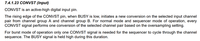
     which says that start CONV pin will initiate conversion for pair


    Which one should I consider. It's not about getting data but we need to minimize the operations.

    Thank you requesting your response

  • Hello,
     We have seen that given two conversion pulse for single pair of channel A and B gives the expected output, but 

    I found one application note named 

    ADS8686S 16-Bit, 16-Channel 1-MSPS Dual Simultaneous-Sampling ADC

    Expanding Analog Input Channels in Grid Applications (Using 16-Channel, 16-Bit, (Rev. A) page 8

     which says that start CONV pin will initiate conversion for pair


    Which one should I consider. It's not about getting data but we need to minimize the operations.

    Thank you requesting your response

  • Hi Rajat,

    Thanks for your post. May I ask what kind of application/project you are evaluating ADS8686S for? I would also like to mention that we recently released a new generation of ADS8686S: the ADS9324. This is a 16-bit, 16 channel ADC in a small 8mm x 8mm package. The ADS9324 also offers differential inputs and true simultaneous sampling. Would this be of interest to you?

    Regarding the issue you are seeing, are you using the software sequencer or the software channel selection registers? In either case, two CONVSTs are needed to output the correct channel data:

    Please consider the datasheet when operating in software mode. The application note you mentioned may be referring to hardware mode.

    Best regards,

    Samiha

  • Hello Samiha,
    1. We are using ADS8686S for Voltage sensing.
    2. No, right now we are not looking for a change.
    3. Software channel selection by writing Channel Select register.
    4. Datasheet also says one conversion pulse will initiate conversion for a pair of select channel in this case A0 and B0 will start conversion on single case but this is not the case.

    5. I have considered datasheet which also says conv pin will initiate conversion for pair of channel A & B.

    Conclusion:
    1. Pair of channel which means A1 and B1 will require two different conversion pulse or not?
    2. Datasheet lacks with this information referring to point 1 in conclusion.
    3. Is there any other solution?

  • Hi Rajat,

    Yes, technically, one CONVST converts the data for a channel pair. However, for the ADC to register the requested channel data, an extra CONVST is needed. For example, in figure 7-13, one CONVST is needed to register that CHx data was requested, and the next CONVST is used to actually convert the CHx channel pair data. This is shown in the timing diagrams.

    Best regards,

    Samiha

  • Hello Samiha,
    Ok, Great.
    I would also like to know how I should calculate the sampling frequency.
    We have set the range to +/- 5V and consider where we are sending two conversion pulse.

    Thanks

  • Hi Rajat,

    Only the sample corresponding to the very first CONVST would not be referred to a requested channel pair (but rather channel 0 pair), every other sample corresponding to a subsequent CONVST will output a requested channel pair sample. So, if I request CHx pair in SDI frame n, CHx pair will be output on SDO frame n+2. The sampling frequency will be the frequency of CONVST, but there will be a latency of 2 frames as explained above and in figure 7-13.

    If using oversampling, the overall throughput of the ADC decreases proportionally with the increase to the oversampling ratio.

    Best regards,
    Samiha