


Part Number: DAC8775
Other Parts Discussed in Thread: ADS8688, TIPD215
Hello.
We need to design a PCB with 2 DAC8775 in a daisy-chain configuration for a total of 8 channel 4-20 mA outputs. The PCB will also contain 2 daisy-chained ADS8688.
The DAC8775 datasheet shows this layer stack-up as an example.
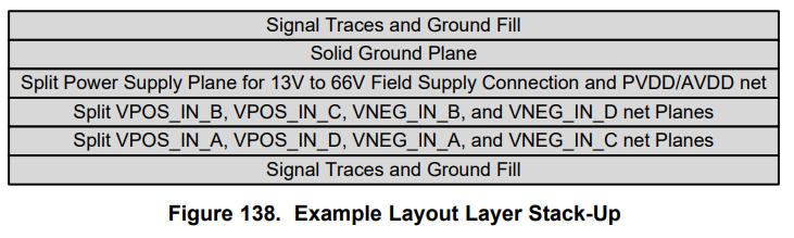
However, the TIPD215 reference design has the split VPOS_IN_X & VNEG_IN_X net planes in layers 2 & 3, and ground & power planes in layers 4 & 5. Here's the PCB layout for the TIPD215.
What are the disadvantages and advantages of these two stack-ups, and why has the latter been selected for the reference design? Is this stack-up recommended for two daisy-chained chips?
Is it feasible to also have the two daisy-chained ADS8688 on the same PCB? I would imagine that the ADS8688 would benefit from having the solid ground plane right under the top layer, as opposed to having it 3 layers away.
We are students and are pretty new to multi-layer PCBs, so we apologize for any mistakes or missing information in the post. We will gladly clarify if need be.
Thanks.
Jeronimo

