Part Number: DAC80504
Hi,
I read the post concerning the DAC80504 SPI Write/Read Operation :
https://e2e.ti.com/support/data-converters-group/data-converters/f/data-converters-forum/956441/dac80504-dac-80504-interfacing-problem-with-tm4c129encpdt-using-spi
However some timings remain unclear,
1) For a write operation, the SPI described in datasheet seems to be a hybride of CPOL=0, CPHA=1 and CPOL=1, CPHA=0.
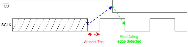
Does SCLK has to be set to '0' at least 7ns before CS falling_edge ?
"tCSIGNORE = SCLK falling edge to CS ignore" : I don't understand the meaning of the definition related to the figure 62 of the datasheet.
Or can it be as following (exemple of write data 0xFF00 to addr 0x02.
The first SCLK edge seen when CS is low is a falling_edge ?
2) For read operation : On the figure 63, on the second part of the diagram during "ANY COMMAND" process, we see that the SCLK seems to be already at '0' after the CS falling_edge, however does the timing is the same for tCSIGNORE.

The first edge seen during the second part of the read process is thus a rising_edge (for data update [see FSDO = '0' in CONFIG Register]) ?
Or can it be as following (exemple of read addr 0x01).

Best regards,
Antoine