This thread has been locked.

If you have a related question, please click the "Ask a related question" button in the top right corner. The newly created question will be automatically linked to this question.

ADS131A04: ADS131A04 configuration issue

Part Number: ADS131A04

Hello everyone,

I'm having a strange issue on ADS131A04.

We already use this ADC in our projects and now I'm testing a new release of my board. 

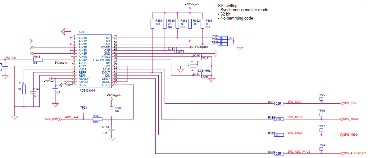
We have made a new redesign of the pcb but the con figuration of the ADC is not changed (at least in theory ...). We use ADS131A04 as a master and with 32 bit transfer size and no hamming code, so M0-M1-M2 are connected to GND-VDD-GND.  

The schematic is not changed:

image.png

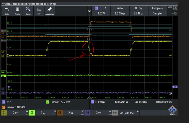
The strange behaviour is that, althaugh the M0-M1-M2, are not changed:

1) in the first case I receive a 32 bit word

image.png

2) in the second I receive a 16 bit word

image.png

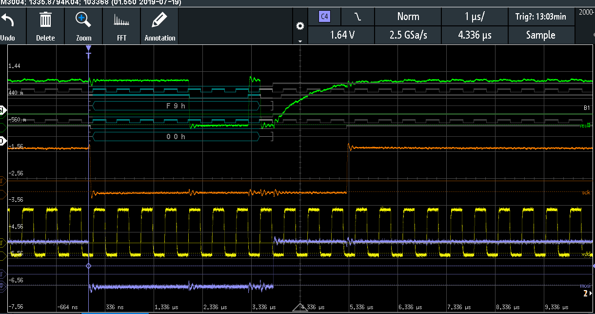
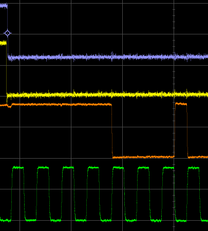
CH1 is CLK (yellow), CH2 is MOSI (green), CH3 is MISO (orange), CH4 is CS (blue).


Resetting the device doesn't change anything.

Any suggestion?

  • Hi suzzi,

    The data from the ADC is 0xFF0400 (MOSI Green) in the first timing, and the second timing shows a similar data (0xFF0400, MOSI Green) but the /CS (/DRDY) was pulled up early. I have few questions:

    1. Were those two adjacent frames?
    2. Were those timings you captured right after the ADC was powered up or reset?
    3. It seems the SCLK frequency in both timings are different, did you change the settings or clock in these two tests?
    4. Was the frame after the 2nd frame always 16-word length?

    It would be good if you could clarify.

    Best regards,

    Dale

  • Hello Dale,

    and thanks for the quick reply.

    The two frame are taken from two different pcb. The first one is working correctly while the second one not.

    Actually the SCLK frequency is the same (the first picture is 2us for division, the second one 1us division).

    That said.

    • Were those two adjacent frames?

    No, they are different pcbs (although with the same schematic..)

    • Were those timings you captured right after the ADC was powered up or reset?

    Yes.

    • It seems the SCLK frequency in both timings are different, did you change the settings or clock in these two tests?

    SCLK frequency is the same but the scale is different

    • Was the frame after the 2nd frame always 16-word length?

    All the frame in the pcb not working are the same. And the device doesnt reply to any command.

    Let me add other stange behaviour.

    I've tried to change the digital settings leaving M1 not connected and to my surprise the word lenght changed to 8 bit!!! that is never mentioned in the datasheet.

    Looks amost like the clock and the data are working with different frequency and the data are coming out twice the speed of the clock.

    In fact I've seen that data are changing at every edge of the clock that is not normal (see the following picture)

    ...

    Matteo

  • In the board that works correcly, the data change just on the positive edge of the clock (and is sampled on the falling)

  • I noticed the clock edge are also smoother in the pcb with the issue.

    Could it be tied to the cristal?

    The model is the same in both pcbs, though.

    I'll check better the oscillation.

  • I've checked the cristal, the frequency seems to be correct in both cases.

    ...

  • Hi suzzi,

    Is the software code running on both PCB boards the same?

    Is the register configuration and initialization the same on both boards?

    Is there any difference between your new design and old design in terms of the circuit and PCB layout? I noticed that  you said the con figuration of the ADC is not changed but I would double check.

    I would suggest you to double check soldering on your new design board, add series resistor between crystal and XTAL2/1 as I have seen significant overshoots on the clocks in the timings you shared.

    BR,

    Dale

  • Hi Dale,

    the FW is the same.

    The point is I can't communicate with the second ADC so every register is on the default state.

    The layout is just slightly different, the main difference is the pcb has 2 more layers on the second design.

    I'll try to put some resistor in serie with the crystal.

  • I finally found out the issue.

    The clk signal had some reflection issue, so on the falling edge the device detected also a rising edge.

    That's why the data was working at double frequency.

  • Adding few picofarad after the serie resistor fixed the issue.

    I guess the title of the topic should be changed.