


Part Number: ADS8354
Other Parts Discussed in Thread: THS4521,
Hi,
we want to use the ADS8354, driven by the THS4521 for one of our upcoming projects (similar to the typical application diagram in the ADS8354 datasheet - see below).
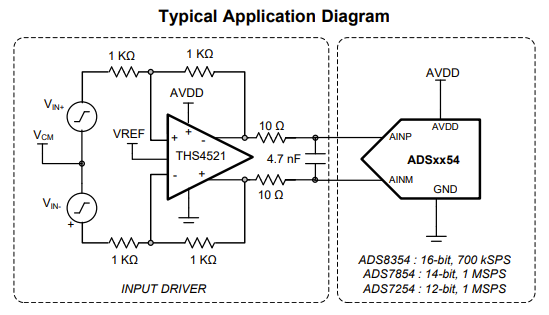
The circuit configuration shall be as follows:
- ADS8354 configured to ±2 x VREF range with internal reference.
- AVDD of ADS8354 and THS4521 supplied from a single 5V voltage source.
- VOCM pin of THS4521 overdriven by a buffer which is connected to ADS8454's REFIO_x pin, in order to set common mode input voltage mid-way of FSR.
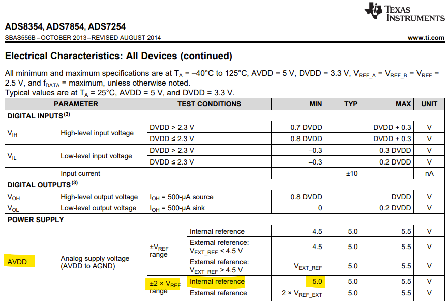
As is stated in the electrical characteristics section of the ADS8354 datasheet (see below), it seems logic that AVDD needs to be at least 5.0V, while VREF is set to the maximum value of 2.5V (REFDAC_x = 1FFh), in order use the full-scale input range.
Now, the actual questions regarding this topic are:
- What happens if the MIN AVDD requirement is not met? Let's assume AVDD drops to 4.95V (for example due to inherent tolerances or load/line transients of the 5V supply). Will there "just" be a clipping of the maximum input voltage range or are there any other "more severe" effects like gain errors, etc.?
- Can the MIN AVDD requirement be relaxed by setting the internal reference voltage to a lower value - for example to 2.40V, which would result in a MIN AVDD requirement of only 4.80V? Or is MIN AVDD independent of the actual VREF setting?
Thanks in advance for your help.
Best regards,
Sebastian

