This thread has been locked.

If you have a related question, please click the "Ask a related question" button in the top right corner. The newly created question will be automatically linked to this question.

ADS1278EVM-PDK: Why Ti engineers split ground planes here?

Part Number: ADS1278EVM-PDK
Other Parts Discussed in Thread: THS4521, ADS1278, THS4551, THS4541, ADS127L01, ADS127L01EVM

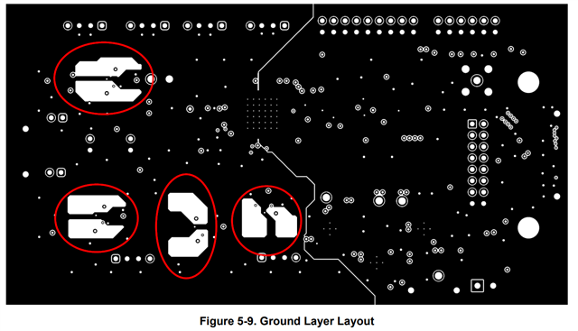
I have very little pcb design background , and i know that spliting ground plane is bad practive and cuts return path , so why did texas instruments ADS1278EVM-PDK engineers cut ground planes under the THS4521 ( I know it's datasheet says so but even this is confusing) , and can I do it in a 4 layer stack without cuting the ground plane safely or is it mandatory , and how about power plane in l3 is it fine to keep the power islands and not cut them or they will also make a problem ? any other ideas of a good stackup for 3 x ads1278 with mcu and sdram and usb 2.0 ulpi , either 4 layer stackup or 6 layer stackup that will preserve a good 24bit signal .. 

  • Hello Soufiane,

    I assume we are talking about the ADS1278V2EVM-PDK, which uses the THS4551.  It is common for high bandwidth amplifiers to remove the adjacent ground plane beneath the negative feedback path for the amplifier.  This removes parasitic capacitive coupling between ground and the feedback path that can cause instability in high speed amplifiers.  The THS4551 (and THS4521) bandwidth is around 150MHz and typically does not require removing ground directly beneath the part, but overall settling time may be improved by removing.  Higher bandwidth parts, such as the THS4541 with 850MHz bandwidth almost always requires removing the ground plane to be stable.

    Basically, for the THS4551 (and THS4521), removing the ground is optional.  We have removed this on many EVMs and left the ground plane in place on others, with similar performance.

    Ideally, a ground plane directly beneath the top and bottom layers is ideal.  If you can afford moving to a 6 layer (or 8 layer) design, then I would recommend using ground planes adjacent to both the top and bottom sides, and then the inner layers can be used for power and signal routing. In the case of the ADS1278EVM, the ground plane.

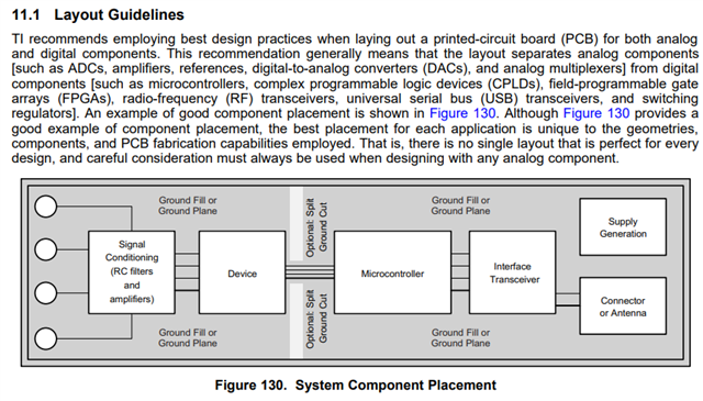
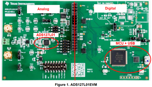
    For best performance, you need to place the digital components separate from the analog components, and make sure digital lines to not directly cross over sensitive analog lines on adjacent layers, or you do not route digital and analog lines next to each other in parallel on the same layer.  For most of TI's precision ADC EVMs, we typically keep the analog on the left side of the board, and the digital on the right side of the board. 

    Take a look at the ADS127L01 datasheet and EVM user's guide, which includes the processor and USB interface on a single board, for a good layout example.

    Datasheet Section 11: https://www.ti.com/lit/ds/symlink/ads127l01.pdf

    ADS127L01EVM User's Guide:  https://www.ti.com/lit/ug/sbau261b/sbau261b.pdf

    Regards,
    Keith Nicholas
    Precision ADC Applications