This thread has been locked.

If you have a related question, please click the "Ask a related question" button in the top right corner. The newly created question will be automatically linked to this question.

using ADS1146 for LVDT application

Other Parts Discussed in Thread: ADS1146, ADS1147

Hi. 

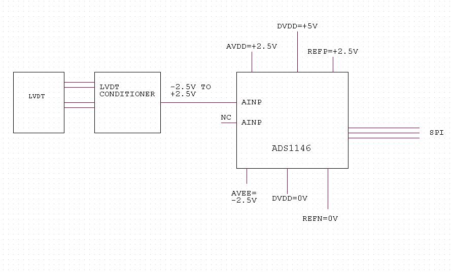
i am trying to interface a LVDT conditioner IC output with ADS1146 ADC. 

the conditioner output varies from -2.5V to +2.5V making it a  single ended bipolar input.

i am going to connect it to AINP pin and going to keep AINN pin open.  the general idea is as follows. 

i just wanted to validate this design from you. Do i look out for some more considerations? 

sushant 

  • Sushant,

    There are a couple of concerns.  First of all, the ADS1146 measures differentially.  This means that one input is measured relative to the other and the difference of the two is the result.  This requires the AINN to be connected, which could be connected to ground.

    Concern number two is the ADS1146 has a common mode input restriction which prevents the device from being able to measure to the supply rails.  Depending on the gain setting you use (which I assume will be 1) the range can be even more restricted.  At a gain of 1, the maximum measurable input will be 0.1V from either rail, so your measurement range will be reduced to +2.4/-2.4 V.

    Best regards,

    Bob B

  • Bob,

    Thank you. 

    i understood the first point but i have some difficulty understanding second point. 

    First let me update the design change. In place of single LVDT output, i am using two LVDTs with ADS1147 as follows. Only one LVDT will be active at a time and internal mux can take care of that channel. now with your help, i have made these changes as shown below. 

    Conditions are as below: 

    AVss = -2.5V, AVdd = +2.5V, PGAgain = 1, RefP = +2.4V, RefN = 0V 

    Full scale input voltage = +/- Vref/PGAGain = +/- 2.4V

    VIN differential = AINp-AINn. [AINn = ground]. so Vin range will be -2.4V to +2.4V. 

    Now the datasheet gives a formula for calculating the common mode input range as 

    {AVss+0.1+[(Vin * PGAGAIN)/2]} < Vcm < { AVdd-0.1-[(Vin * PGAGAIN)/2]}. 

    I am seem to be confused about this calculation. 

    I referred to below design note 

    http://e2e.ti.com/support/data_converters/precision_data_converters/w/design_notes/input-voltage-range-requirements-for-the-ads1248-and-ads1148-families.aspx

    This note refers to maximum expected differential voltage to be used as VIN. it is +2.4V. Hence VCM = 1.2V

    The answer for above equation comes as -1.2 <VCM < 1.2.

     I seem to be missing something very elementary here. 

    regards,

    Sushant 

  • Sushant,

    There are a couple of different ways of looking at this.  One is strictly as differential inputs where the +/- inputs can be of any value between the supplies.  The range where the valid readings can take place is the common mode input range.  There is some point where you can read above and below the common mode within this range.

    Another way of looking at this is setting the common mode point, where you set your range around the common mode point.  In your case you set the common mode to ground which is actually mid-supply and is the best case scenario.  Your full-scale range (Vin) is really +/- 2.4V.  As you know what the common mode point is the range will be the full-scale range of 4.8V in the formula which leaves +/- 2.4V from ground (the common mode).

    I think the part you were missing was the possible full-scale range is different than the input you will provide which is actually 1/2 of the full-scale range.

    Best regards,

    Bob B