Part Number: ADS127L18EVM-PDK
Other Parts Discussed in Thread: ADS127L18
Hello,
we are using a ADS127L18EVM-PDK evalboard that we are interfacing with a stm32h753 instead of the PHI board. Our configuration settings are as follows:
- GEN_CFG1 = 0x01
- GEN_CFG2 = 0x04
-
GEN_CFG3 = 0x08
-
DP_CFG1 = 0x50
-
DP_CFG2 = 0x00
-
CLK_CFG = 0x00
-
CHx_CFG1 = 0x00
-
CHx_CFG2 = 0x01 (channel 0-3)
-
CHx_CFG2 = 0x21 (channel 4-7)
As you can see from the config we only need/use 4 channels. Hence we only have DOUT0 connected to the stm32's SAI. DOUT1 is left floating.
Our usecase is that we typically want to start conversions (via SPI command to CONTROL register) and then keep the ADC running for several minutes. During that time we stream the data via ethernet to a raspberry pi where the data is also visualized.
The START pin is connected to GND as suggested in the datasheet. As a result we are never (re)synchronizing conversions.
The problem we observe is that we always get random errors and the conversions are stopped. The errors also occur when the adc is stopped. If errors occured during stopped condition a subsequent start was ignored. Sometimes the error is visible in the STATUS register (as value 0x02). However, most of the time the STATUS register remains at 0x0. As a workaround we always clear the STATUS register when starting conversions. Now start always work, but the problem that ongoing conversions are stopped upon an error condition is still present. These errors occur independently on two separate devices in different offices.
We also made use of the GUI that is delivered with the ADS127L18EVM-PDK (with the PHI Board). We configured all the control registers to the same values as described above. Unfortunately the working principle of the PHI/GUI is completely different. Nonetheless, we tried to understand it. But we really can't.
Here are the logic analyzer results we see, when we capture 2 samples (D0-D3 are SPI; can be ignored). Single trigger on FSYNC after pressing capture button in GUI.
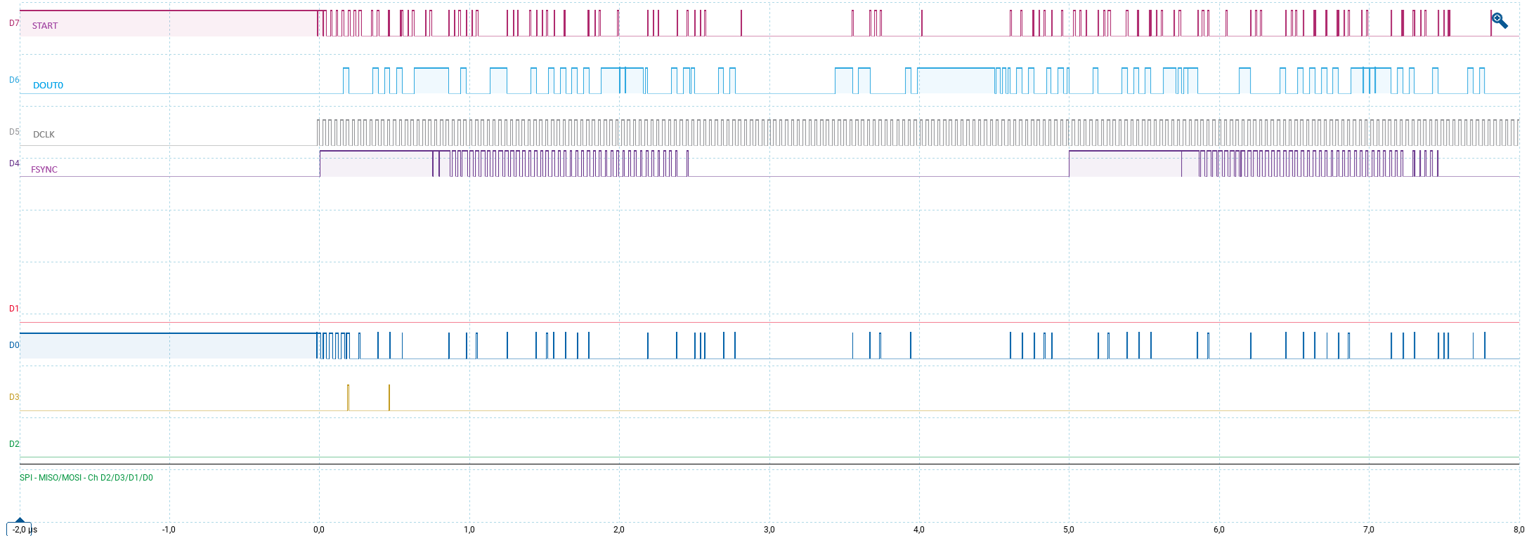
According to my understanding there are continuous restart conditions and also the fact that FSYNC and DCLK look nearly the same at times, doesn't make sense to me.
Even if we would not use TDM there should be 32 DCLK cycles within 1 FSYNC cycle, or? With 2 data lanes (TDM=4), there should even be 128 DCLK cycles.
Do you see an obvious problem in the way we are using the adc? Could you help us to understand the working principle of the GUI/PHI code? Any help would be highly appreciated.
Best regards,
Peter