Part Number: ADC3660
Hi TI Team,
We are designing a system using the ADC3660 and have a question regarding the initialization sequence and the REFBUF pin configuration.
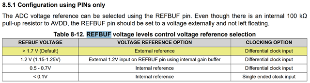
According to the datasheet, during the initialization phase, the device requires a valid sampling clock based on the High/Low status of the REFBUF pin to perform the internally calibration.
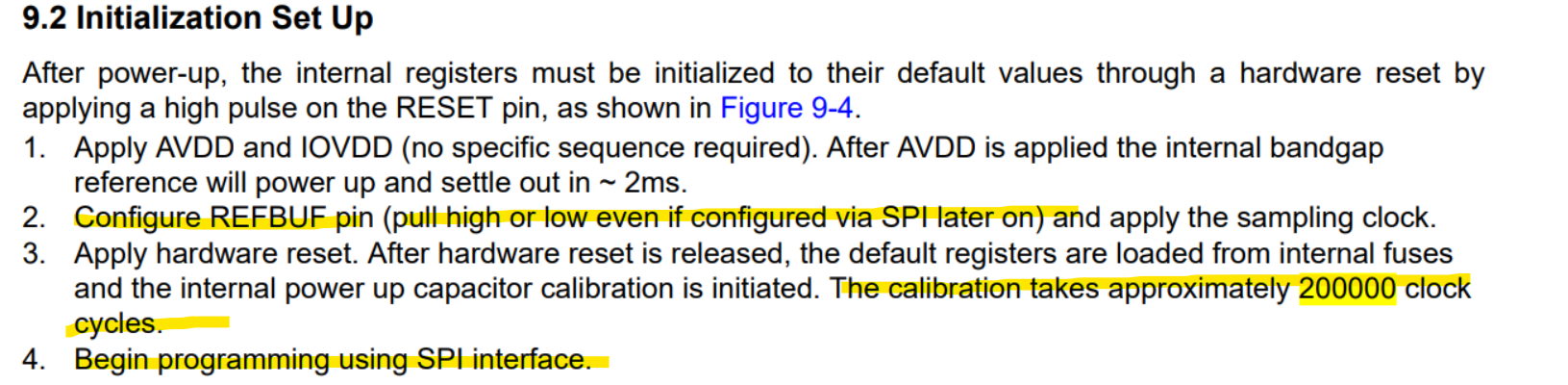
In our application, we configure the sampling clock into Single-Ended mode via SPI after power-up. However, at the very beginning of the power-up/reset cycle (before the FPGA can write to the SPI registers), the clock provided to the ADC is already a Single-Ended clock.
Could you please help clarify the following questions:
-
Does this mean we must hardwire the REFBUF pin to LOW to ensure the device correctly recognizes the Single-Ended clock and completes the internally calibration?
-
If we leave the REFBUF pin floating, will it affect the calibration results?
Thanks and best regards,