ADS114S08: Reading unipolar values

Part Number: ADS114S08

Have the ADS114S08 designed into a unit.  Everything appears correct.  Chip operates very well.

Using a unipolar Avdd supply of +5v with Avss at ground.  AinCOM is connected to the analog ground plane.

I can read voltages up to the 2.5v reference value, but not above.

Are there any programming oddities I need to handle in order to ready 0-5?

I have the PGA disabled and bypassed.


Thank you-

David Dudley


  • Hi David,

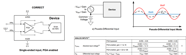
    You can use the pseudo-differential input configuration to drive ADS114S08 analog inputs as shown below. Hold the AINxN pin at a common voltage, preferably at mid supply that is 2.5V in your design. Swing the AINxP pin around the common voltage –VREF / gain to the common voltage + VREF / gain and remain within the absolute maximum specifications, the full-scale range is 0V to +5V when the Gain is 1 and VREF is 2.5V. Verify that the differential signal at the minimum and maximum points meets the common-mode input specification discussed in the PGA Input-Voltage Requirements section in ADS114S08 datasheet.

    BR,

    Dale

  • So... forgive my interpretation of this if I'm wrong, but it seems to me what you're telling me is to hold the AINCOM pin (which is common to all the channel inputs) at 2.5V, which is the reference voltage.

  • It is ashamed that using the reference voltage was omitted from the input multiplexer.  Would have made this a software change, and would have also given a way to be able to read the reference voltage independently.

  • Hi David,

    There are several solutions to configure pseudo-differential input on ADS114S08:

    1. The REFOUT pin on ADS114S08 provides the buffered 2.5-V internal voltage reference output that can be used to bias external circuitry, you just need to route REFOUT to AINCOM on your circuit board.
    2. The ADS114S08 provides an internal bias voltage generator, VBIAS, that is (AVDD + AVSS) / 2 by default. The bias voltage is internally buffered and can be established on the analog inputs AINCOM setting the VB_AINC bit to '1' in the sensor biasing register (08h) without a hardware change.
    3. You can use any precision 2.5V voltage as the bias voltage on AINCOM if it is available on your circuit board.

    ADS114S08 always converts the differential voltage between analog input pins (AINx and AINCOM), it provide 16 bits of data in binary twos complement format, so a positive full-scale input [VIN ≥ (+FS – 1 LSB) = (VREF / Gain – 1 LSB)] produces an output code of 7FFFh and a negative full-scale input (VIN ≤ –FS = –VREF / Gain) produces an output code of 8000h. The output clips at these codes for signals that exceed full-scale. When using pseudo-differential input configuration for your 0~5V single-ended input, the conversion code between 0000h and 7FFFH represents your input voltage between 2.5V and 5V,  the conversion code between 8000h and 0000H represents your input voltage between 2.5V and 5V. 

    Please let me know if you have any other questions.

    BR,

    Dale

  • Solution #2 here would have been great, except I’m using more than 6 inputs.  Current plan is next board redesign will route AINCOM to the REFOUT pin.

    David