


Part Number: ADC34J25
Hi Ti support,
We find a problem when we use the date convert device ADC34J25.
For the input matching of ADC34J25, we copy the demo board design as below. And Our input signal is 64MHz +/- 5MHz. at X29.

But we found the insersion loss for this matching stuff is around 9dB. This is not be accepted by our design. Therefore, we plan to do some modification about this part.
The plan is to keep L177 and L178, and then use the following low pass filter to replace the components before ADC chip input. This LPF we design for 100ohm differential. Is it ok?
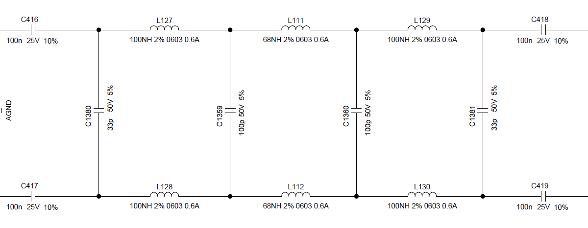
The problem is how to design Vcm connection for the INP/INM of ADC34J25?
Is there any requirement for impedace transform between the above LPF filter and INP/INM ports?
From the datasheet, it seems we cannot omit Vcm connection for the INP/INM pin.
Thanks for your time to support us.
Best Regards,
Brooke