ADC3660: ADC configuration issue

Part Number: ADC3660

Dear engineer,

I encountered some issues while configuring ADC3660. Please help confirm. Thank you.

Usage mode:
(1) AB's 2-channel input
(2) 2-wire output
(3) 16 bit output mode
(4) Binary complement format
(5) Clock Description: ADC_CK: 10MHz; DCLK_IN=40MHZ
(6) Timing diagram

Configuration process (SPI readback is normal).

Reset=1;

Usleep(1000000)

Reset=0;

spi_write_adc_reg(0x0007, 0x4B)// 2-wire bypass 16-bit

spi_write_adc_reg(0x0013, 0x01); usleep(50000);

spi_write_adc_reg(0x0013, 0x00); usleep(10000);

spi_write_adc_reg(0x000A, 0x7F)// 2-wire

spi_write_adc_reg(0x000B, 0xEE);

spi_write_adc_reg(0x000C, 0xFC);

spi_write_adc_reg(0x0018, 0x10);

spi_write_adc_reg(0x0019, 0x12)// bypass 2-wire FCLK 

spi_write_adc_reg(0x001B, 0x88)// MAPPER EN + 16bit

spi_write_adc_reg(0x001F, 0x50);

spi_write_adc_reg(0x0024, 0x00)// bypass, DDC

spi_write_adc_reg(0x0025, 0x00);

spi_write_adc_reg(0x0027, 0x00);

spi_write_adc_reg(0x002E, 0x00);

spi_write_adc_reg(0x0026, 0x00);

spi_write_adc_reg(0x0011, 0x00);

Problem: It has been found that there is an issue with the FCLK output. By default, 0X20, 0X21, and 0X22 are not configured to output. After configuration (0X02=0X00, 0X21=0XF0, 0X22=0X0F), the duty cycle is not 3:1, and there is also a high level of CLK during the low level period.



  • Hi,

    Thanks for the details — I traced this to register 0x21.

    For 2‑wire SCMOS mode, the FCLK pattern registers (0x20/0x21/0x22) should be left at their default reset value (0xFFC00 → 0x20=0x00, 0x21=0xFC, 0x22=0x0F). Per the datasheet (Table 8‑9, step 8 / Table 8‑32), these registers only need to be changed for 1‑wire or 1/2‑wire interfaces — 2‑wire mode always uses the default pattern, regardless of resolution or bypass/decimation setting.

    Your configuration (0x20=0x00, 0x21=0xF0, 0x22=0x0F) reconstructs to pattern 0xFF000, which is actually the correct value from Table 8‑32 for 1‑wire, 16‑bit, real decimation mode — not your 2‑wire bypass setup. Since this pattern is shifted out in sync with the internal serialization clock, applying a pattern meant for a different lane count/serialization factor misaligns the FCLK edges, which explains the skewed duty cycle and the unexpected high pulse during what should be the low period.

    Fix: Remove the writes to 0x20/0x21/0x22 altogether. No FCLK pattern changes are needed for your 2‑wire/16‑bit/bypass configuration.

    Separately (not related to this bug): since your ADC sampling clock is 10 MHz (≤ 40 MSPS), we recommend setting DLL PDN = 1 (register 0x11, bit 2 → write 0x04 instead of 0x00) per Table 8‑1. This extends the acquisition window from TS/4 to TS/2 and improves SNR at lower sample rates.

    Please let us know if FCLK looks correct after this change.

    Regards,

    Samba.

  • Hi,

    Any update? We would like to close this case on priority.

  • Hello,

    updated:

    I used the above configuration but encountered the following issues during testing:
    Configure the 0X14, 0X15, and 0X16 registers to output 0X4000 for testing, but there may be an issue of alternating 0X4000 and 0X4040 outputs. However, using all 0s and all 1s for testing is not a problem.
    SPI_Write(0x14, 0x04); // CUSTOM PAT[7:0] = 0x04
    SPI_Write(0x15, 0x00); // CUSTOM PAT[15:8] = 0x00
    SPI_Write(0x16, 0x48); //Both A/B channels are RAMP (TI E2E only tests A channel with 0x08)
    The waveform tested after outputting the 0X4000 test configuration: DA5 has all zeros, and DA6 is theoretically 0b10000000 → 0b10000000,
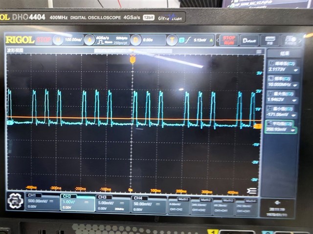
    But in reality, it does cycle like this: 0b10000000 → 0b10001000 → 0b10000000. Below is the waveform diagram of DA6.

    The waveform for capturing DCLKIN is as follows

  • Hi,
    With the corrected
    Constant Pattern config (0x14=0x00, 0x15=0x40, 0x16=0x6C), for output value 0x4000

  • Hi Sambasiva,

    1.During ADC testing, no data sampling was performed. Set the DCLKIN frequency to 8MHz and expect to output the same 8MHz DCLKOUT and 2MHz FCLK with a duty cycle of 40-60%; The test input data is (0x14=0x00, 0x15=0x40, 0x16=0x6C), and the expected DA output is a fixed 0X4000.

    Main issue: Currently in data testing mode, the duty cycle of FCLK is incorrect (mostly high level), and a cycle of high level will occur at low level moments; The DA output is a loop of 0X4000 → 0X4040 → 0X4000 → 0X4040.

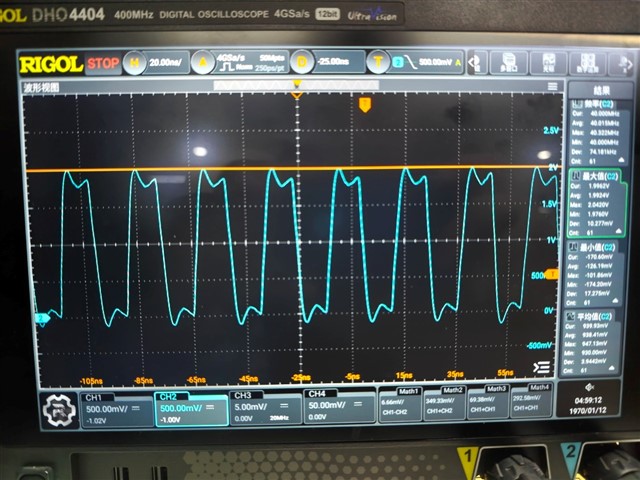
    Figure 1: FLCK (blue) and DCLKIN (yellow) waveforms

    Figure 2 FLCK and DA6

    Figure 3 Hardware Design Schematic

    There is no internal reference used in the register configuration, but an external reference of VREF is used. However, REFBUF and AVDD are powered on together without a 2ms delay. What impact does this have on the ADC state? Is it related to the phenomenon we encountered?

    2. Test results and questions

    When the ADC is not working, the DCLKIN clock signal level output by the FPGA is 1.8V, and there is no overshoot or ringing. After the ADC is powered on, the DLCKIN level is pulled up to 2.1V (the DCLKOUT and FCLK levels are also the same). Subsequent adjustments to the FPGA program have reduced the IO drive capability from 16mA to 4mA. The overshoot issue has been improved, but the ringing is still noticeable. Is this phenomenon abnormal? If there are any abnormalities, can you provide solutions or optimization ideas?

    Figure 4 Overcharging and Ringing of DCLKIN

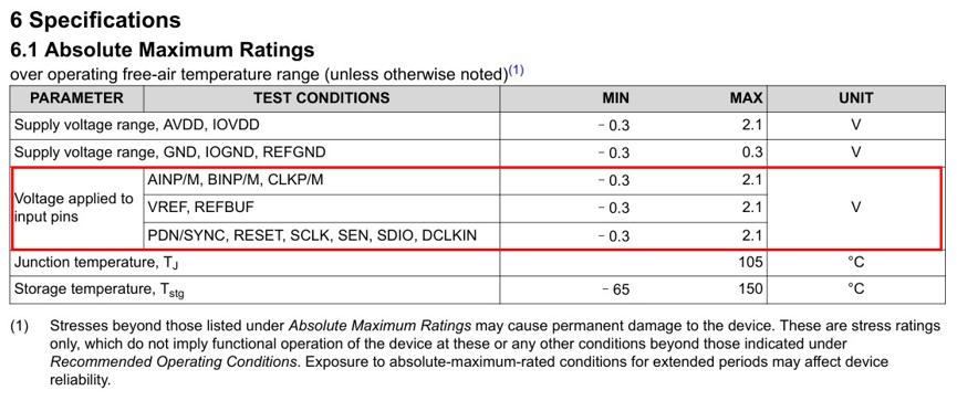
    Will DCLKIN overshoot slightly beyond the pin range of 2.1V (or -0.3V) cause logic problems and affect digital signal output?As shown in Figure 4.

    Does the data manual require the logic level of DCLKIN to be set to 0 below 0.1V and set to 1 above IOVDD-0.1V? Tests have shown that during the ringing process, the voltage level may sometimes be slightly lower than 1.7V (with IOVDD set to 1.8V) or higher than 0.1V. Will this cause logic problems and affect digital signal output?

    3、 Consultation on opinions
    1. In our testing, the DCLKOUT logic read by the FPGA is normal. Can this indicate that the DCLKIN read by the ADC chip is normal? Can the abnormal output of FCLK and data indicate that DCLKIN is abnormal? Or is there any other reason?


    2. The level and jitter requirements for DCLKIN are very strict in the data manual. If they are not met, will it have a significant impact on the data output? Does it match the problem we encountered?


    3. Are there any recommended pin allocation, clock scheme, power design, or interface configuration suggestions for similar application scenarios? Is there any public case or recommended solution from other clients in similar applications that can be used for reference, subject to confidentiality?

  • Hi,

    t1 is mandatory (it's the bandgap settling time, independent of REFBUF drive method), and it's automatically satisfied by waiting — you doesn't need to "engineer" a discrete 2 ms timer on REFBUF itself; you just need to ensure RESET isn't asserted until at least t1 (~2 ms) after power-up, REFBUF to be a stable logic level, and then t2 (100 ns) after that stable level, RESET can go high.

    The ADC3660 requires an external serial clock input (DCLKIN), which is used to transmit the data out of the
    ADC along with the data clock (DCLK). The phase relationship between DCLKIN and the sampling clock(Fs) is
    irrelevant but both clocks need to be frequency locked.

    Regards

    Samba.