Part Number: DAC5674
DAC5674: Clock inputs doubts
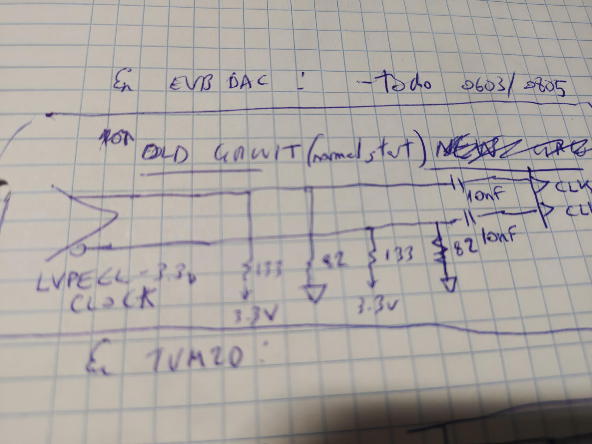
I have used this DAC before without problem. I used an LVPECL-3.3V 200MHz differential clock (DC coupled, with 50 ohm load using resistances to 3.3V of 132R and to GND of 82R terminations) from the LVPECL 3.3V clock generator. For this purpose, the DAC AVDD and CLKVDD (and not IOVDD as another post in the forum says incorrectly) are set to 3.3V.
Really, the coupling to the DAC is finally AC with capacitors because CLK and CLKC pins are self-biased. What is DC coupling was from the clock to the terminations. Maybe I could have used AC as well in that case, but this way worked fine.
After the years, I need to use the same DAC again to redesign the system, and I planned to do exactly the same this time, but I cannot, due to a special behaviour of the DAC clock cenerator chip.
I configure the output for LVPECL and supply it with 3.3V.
But the clock behaves in a special way: before it is programed (via I2C) from our processor, it delivers a DIFFERENT signal in this output. It delivers differential LVCMOS. As the supply is 3.3V for the "permanent" LVPECL 3.3, the clock arriving the DAC will be difefrential LVCMOS 3.3V.
It means "1" = 3.3V in the direct line and 0V in the negated line, and the oppisite for "0".
This has at least two problems, I think I can manage, but some doubt still remains.
One is the currents of a circuit designed for small swing and medium-DC values LVPECL, when the input is LVCMOS (rail to rail) instead.
Two, the AC currents with so large swings
Three, possible DAC max ratings. Not in each pin (0 to CLKVDD=3,3V or bit more), but differentially, since LVCMOS 3.3V presents alternatively +3.3 and -3.3V i.e 6.6Vpp differentially.
I think I can solve the 2 first problems:
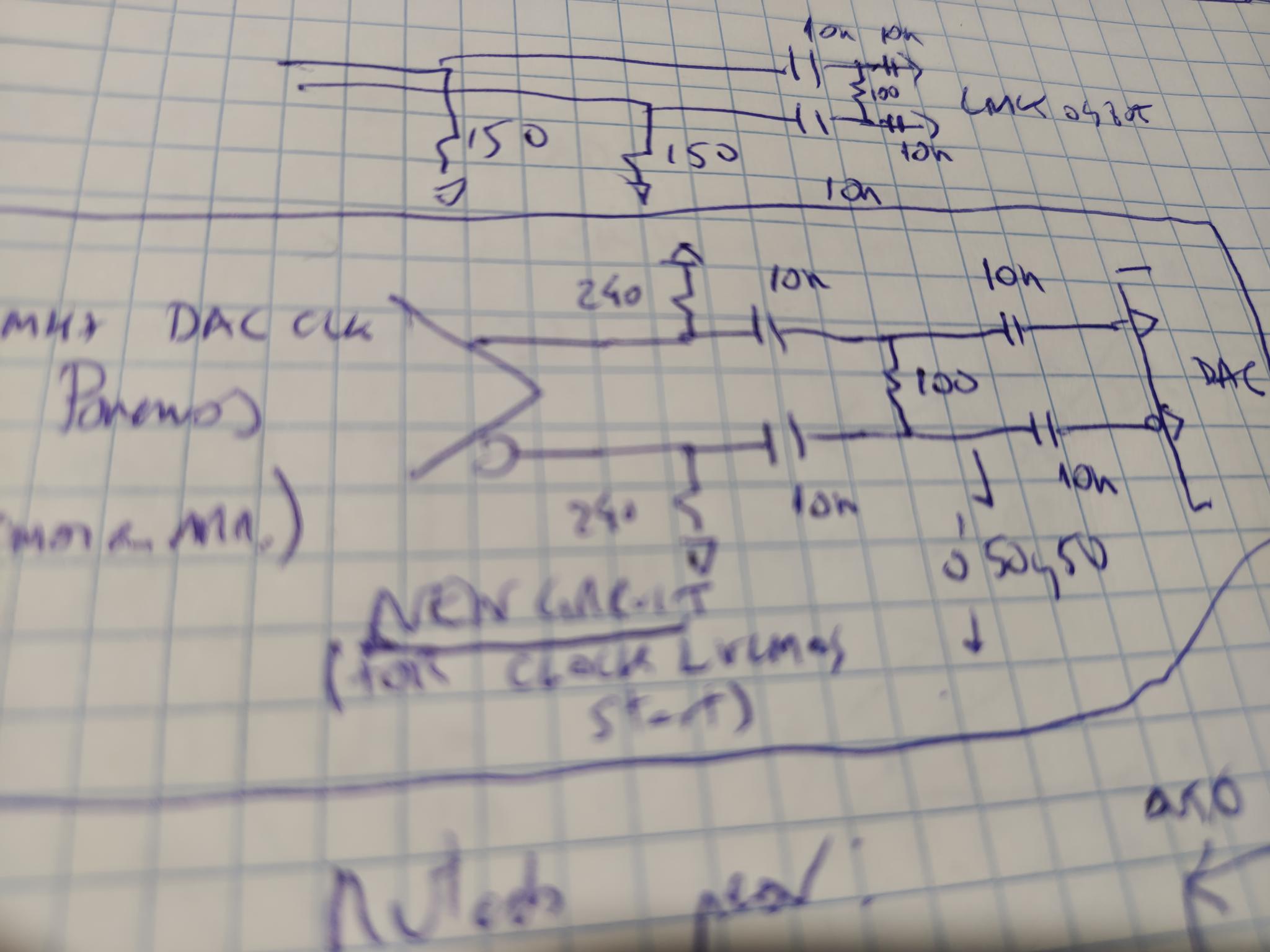
First, I change the DC coupling to AC because otherwise the DC current with 3.3V swing in every line in the start up would ask big currents.
I use 150 ohm resistors to GND just at the clock end as I have done very often with LVPECL sources, TI included, then I insert one 10nF capacitor in each line, and nearthe DAC I load the differential line with a 100 ohm shunt resistor. Finally, other two capacitors to input in AC to the DAC isolating from the internal self bias.
I have cheked the clock behaviour with this load (always with 3.3V output buffer supply), and what it does during the start up LVCMOS "phase" is that it reduces the output swing to about 1.6V, with logical levels 0.6/2.2V. The reduction is pacific and stable and helps to reduce the total differential swing which is extraordinariy large in ths phase compared with the LVPECL final phase.
So instead +3.3/-3.3V the signal reaching the DAC clock inputs has now (with the described circuit) no DC, and a diferential swing of +/-1.6V, which isinto the 0 to 3.3V rails.
What I am not totally sure is, is there any problem entering to the DAC with this clock during the irregular clock LVCMOS output phase, without changing the circuit (allowing the 0/3.3 and 3.3/0V differential clock arrive to the DAC)? In principle I think it is better to avoid it anyway.
Also, to be sure that the circuit I described looks OK for the two phases, when the clock delivers initially LVCMOS 3.3V differential and when once programmed goes to LVPECL3.3V. I am near totally sure that for LVPECL is OK, but your comments will be of help.
The one in the left is the OLD diagram in a system produced for many years is in the left, for pure LVPECL as the clock did not do nothig irregular in the start up.
The one in the right is the circuit I am considering to cope with the initial phase when the generator delives LVCMOS 3.3V. Once programmed it becomes standard LVPECL 3.3V.
Thanks in advance for any comment or data.
JM