This thread has been locked.

If you have a related question, please click the "Ask a related question" button in the top right corner. The newly created question will be automatically linked to this question.

ADS1247: cannot write to the registers

Other Parts Discussed in Thread: ADS1247

I have checked the forum but could not find any answer to my issue.  Here is the problem:

1.  I can read from the registers and they show proper default values.

2.  I can read the ADC conversion results.

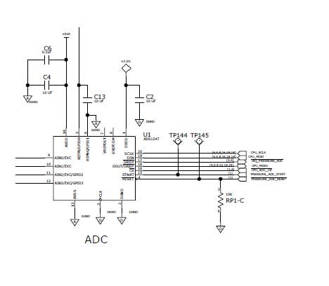
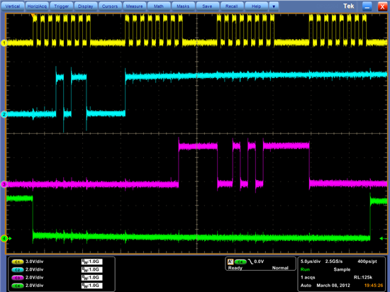
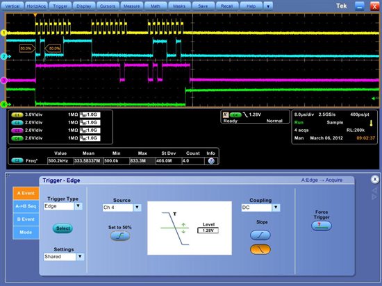
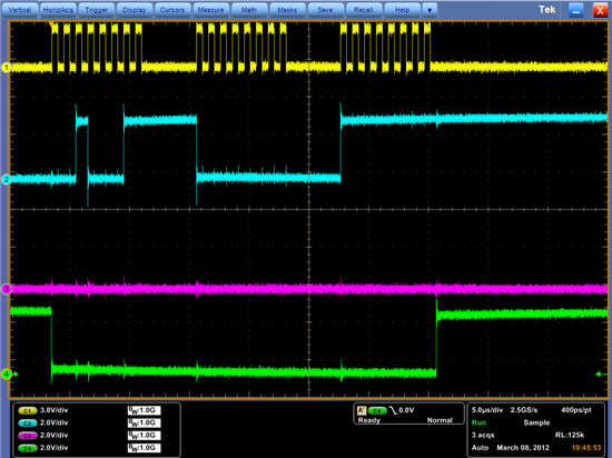
3.  I have check and verify all SPI signal & timing.

4.  I have followed proper steps to set the start pin to high, wait for the current conversion to complete, stop continuous read conversion mode, flush out output buffers,

5.  But I still can not write to the registers.  Despite changing PGA and data rate, I always get default PGA of 1 and 2sps conversion rate.

Is there any timing required between setting start pin high and first write to the chip?

Any insight into this problem is highly appreciated.

Trac

  • Hi Trac,

    Welcome to our Forum!  Can you tell us what sort of controller you are talking to the ADS1247 with?  Are you using your own hardware or the EVM that's available through TI?  If its your own hardware, can you provide perhaps a schematic and a screen shot from your oscilloscope or logic analyser showing your communication sequence?

  • Trac,

    If you can read from the device you should be able to write it as well.  The only issue with writing is if you are in RDATAC mode your communication can be invalid if the conversion result is posted during the write communication.  You must make sure that the write is completed between conversion updates, or you should enter SDATAC mode which stops the automatic posting of results to the output register.

    As Tom mentioned, pictorial shots of the communication will help us.  I might also be able to tell what might be happening from a code snippet of the write transaction.

    Best regards,

    Bob B

  • Thank you all for responding to my questions.

    The microcontroller I use is a ColdFire MCF5328.  The SPI controller is on chip.  Here is the schematic


    Here is the control code:

      // set start pin to high
       enable_register_access();

       // first need to stop reading continuously
       spi_tx_buffer[0] = 0x16;   // stop channel 1 continuous conversion reading
       spi_tx_buffer[1] = 0xFF// bogus data read to clear out buffer
       spi_tx_buffer[2] = 0xFF// bogus data
       spi_tx_buffer[3] = 0xFF// bogus data
       qspi_driver.write( config, spi_tx_buffer, 4);
       pressure_adc_queue
    .get((void *)&spi_rx_buffer, RTOS_WAIT_FOREVER);
       ads1247_org_buffer[
    0] = spi_rx_buffer[2];
      sleep(300*TIMER_TICKS_PER_MILLISECOND);

       // testing
       // ADS 1247 set up mode: programmable gain amplifier and conversion rate
       spi_tx_buffer[0] = ADS1247_WRITE_REG | ADS1247_SYS0_REG;    // write to reg SYS0
       spi_tx_buffer[1] = 0x00;                                    // num bytes-1
       spi_tx_buffer[2] = ADS1247_PGA_GAIN_128 | ADS1247_DATA_RATE_20SPS;    // Data rate = 20SPS
       qspi_driver.write( config, spi_tx_buffer, 3);
       pressure_adc_queue
    .get((void *)&spi_rx_buffer, RTOS_WAIT_FOREVER);

      // read back result to confirm
       spi_tx_buffer[0] = 0x20 | ADS1247_SYS0_REG;  
    // read from register SYS0
       spi_tx_buffer[1] = 0x0;   // number of registers to read - 1
       spi_tx_buffer[2] = 0xFF// bogus data
       qspi_driver.read( config, spi_tx_buffer, 3);
       pressure_adc_queue
    .get((void *)&spi_rx_buffer, RTOS_WAIT_FOREVER);
       ads1247_final_buffer[
    0] = spi_rx_buffer[2];

      // set start pin to low
       disable_register_access
    ();

    Here are the pictures of the SPI timing
    The yellow channel is the SPI CLK.  The blue channel is MOSI, the purpose channel is MISO, and the green channel is the chip select

    Firt SPI timing is where write SDATAC and three dummy reads to clear the buffer.  The seconnd SPI shows write to register 0x3, and the last SPI timing shows read from register 3 (all zeros).


    Again TIA, Trac

  • Trac,

    On the schematic I noticed that you do not have a cap on VREFOUT/VRECOM.  You should place a cap to reduce noise.  That is not causing your write problem however. One thing to keep in mind is SDATAC does not take effect until after the next conversion result completes after the command is issued.  Some data is coming out of the ADS1247 during the write which leads me to believe there is something still going on.

    I suggest waiting until the conversion result completes after SDATAC is issued before writing to the registers.

    Best regards,

    Bob B

  • Hi Bob,

    Thank you for pointing out the design error with reference to VREFOUT/VREFCOM.  We use the internal reference to miss out glaring notice in the data sheet.  In fact, we have already been updating the design to add some capacitance between VREFOUT/VREFCOM.

    On the other note, the code does have 300 milliseconds sleep after issue SDATAC command to make sure any going conversion to complete before write to or read from the registers.

    Trac

  • Trac,

    Do you read the last data after the SDATAC, or do you just wait and then write?  In theory you could do both at the same time (read out the data and write the registers).  I am wondering if the SDATAC command is actually taking place.  Is is possible to monitor DRDY to see if there is a conversion result taking place at about the time you are writing?

    Another possibility is there is an issue with the DIN signal, have you probed the ADS1247 device pin to verify that the signal is getting to pin?

    Best regards,

    Bob B

  • Hi Bob,

    To answer your questions.  I do not wait but write immediately after set START to high.  At power up, the chip was held in reset as the START was low.  After we un-reset the chip, I wait for 10 ms.  The chip is in sleep mode since START pin is low.  Then I set START pin high to enter read/write register mode and start the conversion.  At 200ms conversion time for 5SPS, I am pretty sure the conversion result still miles away when it was written to or read from the registers.  The fact that I can read the registers and conversion result indicates that DIN should be valid.

    BTW, I have solved the problem.  Actually, there is 2 issues.  The first one is our mistake with regarding the CS signal.  In our design, the CPU is controlling 28 SPI devices.  The CS signal decoding logic has a bug that generates the same CS for 2 differenct devices.  Ahem! that is the core of the problem.  The second is a peculiarity with this chip.  It seems to require to complete at least one conversion completed, then the internal chip's state machine will get into proper state (in sync) for the write and read registers.  When the chip signals the conversion ready, you can immediately read out the conversion result to clear the output buffer then continue with write and read the registers.  Someone at TI or the designer of this chip should shed some lights on this simple yet mysterious transaction between SPI bus in synchronization with the internal control.  An App Note would save us tons of time.

    Again, thanks for all the responses and tips.

    Trac