This thread has been locked.

If you have a related question, please click the "Ask a related question" button in the top right corner. The newly created question will be automatically linked to this question.

Unable to read data from ADS1258

Other Parts Discussed in Thread: ADS1258

Dear TI Employee & members,

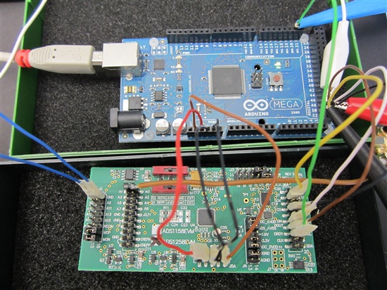
I am currently working on a project to interface ADS1258EVM board to Arduino Mega2560 via SPI interface (SCLK, MISO,MOSI,CS).

I have tested the ADS1258EVM board with MMBO DSP kit and it works fine.

Now I have removed the ADS1258EVM board from MMB0 and connected it to the Ardunio MEGA2560.

Jumper settings are as follows:

1) J5.3 (+5VA) connected to +5V of Arduino.

2) J5.5 (DGND) and J5.6 (AGND)  to GND.

3) J5.9 to +3.3V.

The jumper settings for J4 are accroding to the figure 3 of Users guide.Aditionally I have measured the currents on the jumper  and they seem fine.

Next,

4) J6.1 (Start ) and J6.2 (PWDN) connected to 5V(High) 

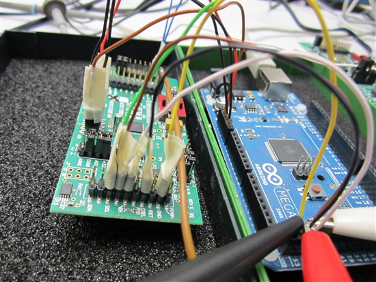
5) J6.3 (SCLK) connected to Pin50 of arduino.

6) J6.7 (CS) to pin53 chip select.

7) J6.11 (DIN) to pin51 (MOSI).

8) J6.13 (DOUT) to pin50 (MISO)

9)    J6.15 (DRDY) to pin2 (interupt).

On J1 and J2 I have connected 16 analog channels of my sensor.

I am using external clock  at 16MHz for SPI clock SCLK.I have programmed the SCLK in code and I am dividing it by 128. So 16MHz/128= 125KHz. Is its fine?Lower limit on clock is I have calculated is 73.5KHz with DRATE=00 (1/1831=546µs, and tsclk=546µs/40=13.6µs >> Freq=73.5KHz) 

The ADS1258 is using its own internal clock at 15.78 MHz. CLKSL pin is attached to GND. 

The register settings are: 

CONFIG0=0x02 ( STAT=1, Bypass=0 internal, Mode=AutoScan)

CONFIG1=0x30 ( DLY=011, DRATE=00 i.e. 1830sps with delay it would be 1730sps)

MUXSXH=0x00

MUXDIF=0x00

MUXSG0=0xFF (All channels selected)

MUXSG1=0xFF

SYSRED=0x00

GPIOC=0xFF

GPIOD=0x00

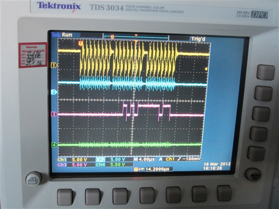
I am usng Channel Data Read format with DRDY indication. In my program I first intialize the pins used for SPI communication and set the frequency (125KHz) and mode3 (Cphase=1, Cpolarity=1) . I have chceked all the combination of phase and polarity, this seemed to me fine as for others I donot see any actvity on the oscillopse. Also I have tried SCLK of 8MHz, 4MHz,1MHz etc and it doesnot make any affect on the output data.

Next I write all of the registers with value above and then try to read ID regsiter. The ID register is giving wrong value. Don't know why? It keeps on taking random value everytime I call it.I am using register data Read command=0B0100 0000 with MUL=0.

Secondly I read Channel data with 0B0011 0000 command for data read, MUL=1. The channel data gives me all the time 0. it seems data channel data read command acts like reset command (0B1100 0000) so it reset the register instead of reading it and give me all the time zero.

On DRDY line doesnot go LOW, it is always giving high. While I am polling for a low value indicating the new data has arrived. 

On output line on oscilloscope I get zero. While I have set chip select to low , and start to high all the time.

I would be highly thankful if someone could help me figure out this problem.

Best Regards,

Faisal

  • Hi Faisal,

    We'll go through your hookup to see what issues there may be hardware wise with your ADS1258 setup.  In the meantime, can you send us screen captures from an oscilloscope showing how you are communicating with the ADS1258?  Is it possible for you to share a schematic with us showing the area around the ADC and it's connections to your controller?

  • Dear Tom,

    Thank you very much for your response.

    Here are the screen shots of my Electronic setup and Oscilloscope:


    Figure1: Electronic Setup (Top)

    Figure2: Electronic setup (Side)

    Jumper settings and wiring:

    1)  J5.3 to 5V on arduino

    2)  J5.5 and J5.6 to GND

    3)  J5.9 to 3.3V

    4) J6.3 to D52 (SCLK) on arduino

    5)    J6.7 to D53 (CS) on arduino

    6) J6.11 to D51 (MOSI) on arduino

    7) J6.13 to D50 (MISO) on arduino

    8) J6.15 to pin2 (INT) on arduino

    9) A0 on J1 is connected to +-2.5V of signal generator (To make things simple to understand I just connected one channel)

    and screen shot from Oscilloscope:

    Figure3: Oscilloscope Screen shot

    Channel1: SCLK (Yellow:  last 24 clocks)

    Channel2: DRDY (Blue-HIGH)

    Channel3: DOUT (Pink)

    Channel4: CS (Green-LOW)

    By changing the SPI frequency (SCLK)  from 125KHz to 1MHz (Master clock=16 MHz) and Mode=11( Cphase=1, Cpol=1) I was able to see something on DOUT. It gives me a constant value of 15F6(HEX) or 5622 (Decimal). I realize my clock is also not so clean.I connected a 50 Ohm resistor before applying to SCLK pin  .Is there any other remedy for it?Also I shorted MUXOUTP and MUXOUTN to ADCINP and ADCINN respectively. I did not use any buffer amplifier.Is it fine? Moreover I set Bypass=0 in Config0 for it.

    The DRDY doesnot change value and it is always high. In my code I changed the DRDY from LOW to HIGH.Now I am continuously reading the data, since DRDY is always high.

    void loop() {
     
     
      // don't do anything until the data ready pin is HIGH:


     if (digitalRead(DRDY) == HIGH) {
     

       //Read the Channel data with channel data read command.get 4 bytes, one status and rest 3 bytes of data


       int channelData = readChannel(READ_COMMAND,4);     // READ_COMMAND= 0B0011 0000 (MUL=1)
     
       Serial.print(channelData,HEX);
       Serial.print("\n");   
      
      
       delay(250);

    }

    As you can see in figure3, I only get two data bytes 15F6Hex or 5622 in decimal, and no status byte while I have set STAT=1 in config register0.Otherwise I could poll for NEW bit. Should I use Start pin to control the loop?


    One thing I didnot understand, in which format is the data coming?.I mean is it my actual data (in Volts or mV) or is it coded in some other form e.g. 2's complement. How to get the actual value in volts/mV?. I am providing +-2.5V sine wave at channel0. while I do not see any negative values of data on COM3 ouput screen of arduino. May be I need to minus some offset value?

    Secondly I want to use all of 16 single ended channels in Auto Scan mode, how do I know which data belong to which channel?

     Later on I connected two channels i.e. A0 and A7 and respectively changed the setting of MUXSG0=0x41. But still values did not change, it gives again 5622, although I have +-2.5V on A0 and +-1V on A7. It seems A7 takes on values of A0. There is some interefence between channels. How to avoid this?

    Thank you very much and have a nice weekend!

    Faisal

  • Hi,

    After disconnecting the pins ST(start) and GPIO0 on J3, it seems I am getting something from ADS1258EVM board but not sure if it is correct.

    I have further connected START pin on J6A on the board to one of interupt pins on arduino, as well as CLKSEL to GND. Moreover SPI mode is changed to 0 i.e Cphase=Cpol=0.

    To make things simple, I am applying analog input voltage of +-2.5 V on the Channel1(A0) only while others inputs (A1-A15) I have disbaled.(MUXSG0=0x01 and MUXSG1=0x00).I will use the other inputs later when i get the correct results.

    I am reading the channel ID=8B and all other registers correctly, which means my board is working. 

    By using channel data read command (register format) with MUL=1, and continuously reading only channel1 , I have obtained follwing values (in decimal):

    -14208

    -14208

    -14209

    -30710

    -14208

    ....

    All the values are negative while I am applying +-2.5 V at the analog input. The values do not seem to be correct. Is this due to something I am still missing on the hardware side?

    Secondly How do I convert the values I get to Voltage?Is there any conversion formula? I am using unipolar supply at AVDD=5V, AVSS=GND, DVDD=3.3V.

    How to know the reference voltage? Is it the same as AVDD=5V ?

    I have noticed with the oscillscope that the when I apply +-2.5V from generator at the analog input of board,it clips the negative values.Why is that?

     Previously when I tested the EVM board with MMB0 DSP kit I alligned S1 and S2 in the center as mentioned in the guide.Now I am not using MMB0 anymore and supply the voltage with my controller .What should be the switches S1 amd S2 position, left or center?

    Please help me solve this problem.I have spent many days on it without much success.

    Thank you in advance.

    Best Regards

    Faisal


  • Faisal,

    Let's take this one step at a time.  It appears that you are trying to drive a bipolar signal into the unipolar supplied ADS1258.  By what you are describing, it would appear that you are going below ground with your input and turning on the ESD diodes.  This can damage the ADS1258 as you are exceeding the absolute maximum input voltage.  Your generator must be generating your input signal above ground, which will require a DC offset of 2.5V.  This will keep the maximum positive peak at 5V and the minimum at 0V.  This assumes that the signal generator ground and the EVM ground are the same potential.

    Best regards,

    Bob B

  • Hi Bob,

    Thank you very much.

    I have now added an offset of 2.5V to the bipolar signal of +/- 2.5 V as you have suggested. But I am still getting a negative number 0xFFFF880A.

    Is it due to something I am still missing on hardware side?

    I have connected unipolar supply of 5V at AVDD and AVSS=GND and DVDD=3.3V.

    How to limit the input voltage into the ADS1258 other than adding offset? As later I want to connect my sensor that gives 16 bipolar signals in the range of +/- 2.5 V directly to analog inputs.

    Best Regards,

    Faisal 

  • Faisal,

    Previously you asked about the S1 and S2 switches.  They should be in the left hand position so that AVDD and AVSS are used as the reference voltage.  The code value you sent back is 32 bit, so I will assume that the MSB is the STATUS byte.  Review the meaning of the STATUS byte on page 33 of the datasheet.  Also realize that the value you gave me is for channel 15 and not channel 0 where you said you have your generator connected.

    Keep in mind that if you are setting up the device to read single ended measurements, you must connect AINCOM. 

    To directly connect a +/-2.5V signal to the ADS1258, you must also power AVDD/AVSS with +/-2.5V.

    Best regards,

    Bob B

  • Hi Bob,

    I am sorry I sent you wrong code. The actual code I am getting is just 880A. The first byte 88=10001000 is the status byte as far as I understood with last five bits being the channel ID=01000=08h so the channel0. And next byte 0A=00001010 is the 8 bit data. It is very strange that I am getting only 8 bit of data instead of 24 bits. This can be confirmed from the screen shot of SPI communication I sent earlier. I can see only 24 clock cycles on  oscilloscope instead of 40 clock cycles for channel data read operation.

    I wonder what could be the problem. Do you have any idea?

    Secondly, I want to ask a couple of questions regarding hardware if you don't mind.

    1) I want to design my own PCB using ADS1258 with 16 input channels. I have seen the circuit diagram of ADS1258EVM board given in the users guide that there are two level translators U11 (SN74AVC2T45DCT) and U12 (SN74AVC8T245RHL) used. What is their function and are they mandatory to connect? For my application I need only SCLK, DIN ,DOUT, and CS. Can I connect these pins directly to my microcontroller board (Arduino Mega2560) intead of using level translators?

    2) Also I want to ask about the Reference inputs(VREFP and VREFN) to the ADS1258.Can they be driven directly with AVDD/AVSS  or an external regulator is required?

    3) ADC will work if there is no buffer amplifier between MUX outputs(MUXOUTP and MUXOUTN) and ADC inputs (ADCINP and ADCINN)? 

    Thank you very much for your help!

    Best Regards,

    Faisal

  • Faisal,

    When using channel data read format, you need to make sure that you are reading the data completely before the next DRDY pulse, or the data returned will be corrupted by the result of the next result.  You also need to be sending 32 clocks, so I think there is something missing in your code. If you are in fixed channel mode (and not scan) then 24 clocks would be appropriate and no status byte is sent.

    Regarding the PCB questions, you don't need the level shifting as long as your micro and the DVDD of the ADS1258 are the same.  You can use the supply voltage as the reference, but remember that a noisy supply will add noise to the reference and that noise will also be added to the result.  The need for a buffer amp depends on the signal being delivered.  You might want to have an anti-aliasing filter, and you can easily add an active one between MUXOUT and ADCIN.

    Best regards,

    Bob B

  • Hi Bob,

    Thank you very much for your answers.It seems I am getting the complete data now.

    You are right, there were some bugs in my code which I have corrected now. I was sending only 16 clocks instaed of 40 clks to converter.

    The converter works well for one channel and I can see correct data coming from COM port. But when I enable all 16 channels with MUXSG0=FF and MUXSG1=FF, I see the converter skips some channels and sequence is also not correct e.g. CH0, CH7, CH15, CH4, and so on. May be there is some delay in my loop perhaps.Don't know yet. I will check it later.

    Anyways, many many thanks for your help!!

    Greeting from Germany.

    Best Regards,

    Faisal