This thread has been locked.

If you have a related question, please click the "Ask a related question" button in the top right corner. The newly created question will be automatically linked to this question.

Interfacing the ADS1255 to the MSP430F5438

Other Parts Discussed in Thread: MSP430F5438, ADS1255

Hello!


I want to connect the ADS1255 to the MSP430F5438 via SPI. After the initialisation of the MSP I want to write to the registers of the ADS. Afterwards I want to read them again to check if the right values are stored.

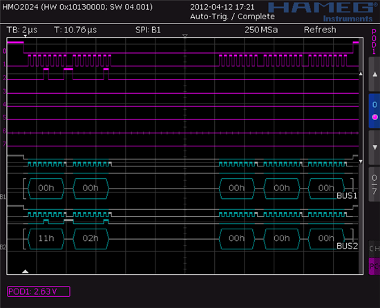
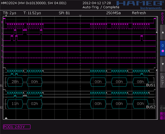
I can see that the right commands and values were transmitted to the ADC using a logicanalyzer.  But when I want to read the registers, the ADC just gives me back a lot of 0x00s or other random numbers but never the values I sent.

SCLK of the SPI is 2.9MHz, four - wire. The inactive state of the clock is low, data is changed on the first UCLK edge (rising) and captured on the following edge (falling).

Here is the code that i use to init the ADC:


P4OUT &= ~0x04;                                    //CS low
UCB3TXBUF = 0x0F;                                //send command to stop sending data continously
while((UCB3STAT & UCBUSY));            //wait until byte is sent
P4OUT |= 0x04;                                    //CS high
    
 __delay_cycles(100);
    
  while(P1IN & 0x04);                            //wait for DREADY of the ADC to get low
  P4OUT &= ~0x04;                                    //CS low
  UCB3TXBUF = 0xFE;                                //RESET
  while((UCB3STAT & UCBUSY));            //wait until byte is sent
  P4OUT |= 0x04;                                    //CS high
        
        __delay_cycles(100);
        
        
        P4OUT &= ~0x04;                                    //CS low
      UCB3TXBUF = 0x52;                                //write command + address of the register - write to 0x02 ADCON-register
       while((UCB3STAT & UCBUSY));            //wait until byte is sent
      UCB3TXBUF = 0x02;                                //(number of registers that will be written) -1
      while((UCB3STAT & UCBUSY));            //wait until byte is sent
      UCB3TXBUF = 0x00;                                //clock out on clk-pin of the ADC is OFF, PGA = 1,
       while((UCB3STAT & UCBUSY));            //wait until byte is sent
      UCB3TXBUF = 0xB0;                                //Samplerate = 2000 SPS
       while((UCB3STAT & UCBUSY));            //wait until byte is sent
        UCB3TXBUF = 0x00;                                //GPIO
       while((UCB3STAT & UCBUSY));            //wait until byte is sent
        P4OUT |= 0x04;                                    //CS high
    
        __delay_cycles(100);
        
        P4OUT &= ~0x04;                                    //CS low
      UCB3TXBUF = 0xFC;                                //send sync-command
       while((UCB3STAT & UCBUSY));            //wait until byte is sent
      UCB3TXBUF = 0x00;                                //send wake-up command
      while((UCB3STAT & UCBUSY));            //wait until byte is sent
        P4OUT |= 0x04;                                    //CS high
        
        __delay_cycles(100);
        
        P4OUT &= ~0x04;                                    //CS low
      UCB3TXBUF = 0xF0;                                //send command to stop send data continously
       while((UCB3STAT & UCBUSY));            //wait until byte is sent
      P4OUT |= 0x04;                                    //CS high
        while((!P1IN & 0x04));                    //wait for DREADY to go low -> calibration completed


Afterwards I read the register continously:

P4OUT &= ~0x04;                                                               //CS low for adc
  UCB3TXBUF = 0x11;                                                       //read command + address of the register
  while((UCB3STAT & UCBUSY));                                      //wait until byte is sent
    UCB3TXBUF = 0x02;                                                       //send number of registers to be read -1 
    while((UCB3STAT & UCBUSY));                                 //wait until byte is received
    __delay_cycles(120);                                                //wait until command is processed
    UCB3TXBUF = DUMMY;                                                  //read content of register
    while((UCB3STAT & UCBUSY));
        UCB3TXBUF = DUMMY;                                                 //read content of register
    while((UCB3STAT & UCBUSY));
    UCB3TXBUF = DUMMY;                                                   //read content of register
    while((UCB3STAT & UCBUSY));
  P4OUT |= 0x04;                                                                     //CS adc high
    __delay_cycles(1000000);


Where is the mistake that I do? Thank you all!

  • Hi J.S.,

    Welcome to the forum!  The code looks like you are sending the RREG command to the ADS1255, starting with ADDR 1, reading one register.  I suppose DUMMY is set up as 0x00 in a header somewhere, so that is fine.  I don't see where you are actually 'storing' the return data though.  I was expecting something like 'Byte2' = UCB3RXBUF.  What do you see in the debugger window if step through the DUMMY transfers? 

  • Hello!

    That's right, i want to read the register using the rreg-command and 'dummy' is a 0x00. Until now I don't store these data because I just wanted to see, if the registers contain the right values.The debugger window shows me the same values the analyzer does.

    Here you can see two screenshots of the data to and from the ADS1255.

    0 -> CS

    1->SCLK

    2->MOSI

    3->MISO

    The data on MISO seem to be random numbers but I logged it (sent the data to the pc and stored them with a terminal program) and all the data consist of "0x00" "0x08" "0x28" "0x40" and "0x94". After a reset of the MC and the ADC the SPI showed the same behavior just with different numbers like "0x50"....

    I also checked my SPI-initialisation but after so many hours in front of my computer I do not see a mistake... (UCCKPL and UCCKPH are changed to '0' when I start the SPI-communication with the ADC)

    {
        
      UCB3CTL1 |= UCSWRST;                                                                                                         // reset UCB3 during setup
      UCB3CTL0 |= UCMST + UCCKPL  + UCSYNC + UCMODE_2 + UCMSB;                       // Data is changed on the first UCLK edge and captured on the following edge.
                                                                                                                                                                // The inactive state is high
                                                                                                                                                                // Master mode
                                                                                                                                                                 // 4-pin SPI with UCxSTE active low: Slave enabled when UCxSTE = 0
                                                                                                                                                                  // Synchronous mode
      UCB3CTL1 |= UCSSEL_2;                        // Clocksource is SMCLK (18MHz)
      UCB3BR0     = 0x04;                                   // Rate = SMCLK/4 = 4,5MHz
      P10DIR   |= 0x0B;                                        // P10.0+1+3 are outputs
      P10SEL   |= 0x0F;                                       // Peripheral function activated for Pin 10.0...10.3  
        
        UCB3CTL1 &= ~UCSWRST;                        // restart UCB3


    }

    Thank you a lot again!

  • J.S.,

    Slow down your SCLK frequency.  See Figure 1 of the datasheet for t1.  The maximum is 1/4th of the master clock frequency.

    Best regards,
    Bob B