This thread has been locked.

If you have a related question, please click the "Ask a related question" button in the top right corner. The newly created question will be automatically linked to this question.

ADS reading is uncorrect when change PGA setting

Other Parts Discussed in Thread: ADS1247

I am using ADS1247 to sample two channel,

Conditions : 
AVDD = +2.5V, AVSS = -2.5V, VREF = 2.5V(to AVSS)
AINP=1.0434V

AINN=1.0327
VINdifferential =  AINP –AINN   = +0.0091V 
VCM = (AINP+AINN)/2 = + 1.03805 V

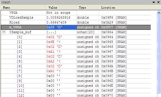
My problem is: circling through two channel,

When I set PGA =0x04,one channel data out is 0x01D4,seems correct,

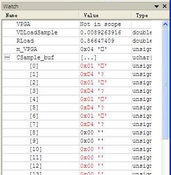
When I set PGA =0x08,data out is wrong,

       VLOAD10MAsample(m_VPGA);//first channel

       IRessample(m_IVGA);//second channel


void VLOAD10MAsample(unsigned char loadPGA)

{

       ReadAIN2();//change mux0

       PGA_SPS_ADS1247(loadPGA,5);//setting PGA and SPS

       OfsCal_ADS1247();//offser calibration

       ADS1247_ContinusSample();   


}

void IRessample(unsigned char loadPGA)

{

       ReadAIN1();

       PGA_SPS_ADS1247(loadPGA,DEFAULTSPS);//setting PGA and SPS

       OfsCal_ADS1247();//offser calibration

       ADS1247_ContinusSample();


}    

please helps.

  • Hi Zhang,

    Assuming that VREFP - VREFN= 2.5V; the reference should be in the allowed range.  The 10mV differential signal and the common mode voltage of 1.0434V should be in the allowed input voltage range with bipolar supplies of +2.5V and -2.5V.

    - Can you please clarify the PGA gain settings, in other words what is meant by PGA= 0x08h or '1000'?  The PGA gain is controlled by the SYS0 register where bits 6:4 (3 bits wide) of the SYS0 control the PGA gain :

    000    PGA=1
    001    PGA=2
    010    PGA=4
    011    PGA=8
    100    PGA=16
    101    PGA=32
    110    PGA=64
    111    PGA=128

    - Can you please clarify the conversion results obtained from the 10mV differential input voltage ?  The conversion results shown on the description are hex 0x01D4 (16 bit wide) which do not seem to be correct.  The device is 24 bit converter; a 10mV differential input at gain of  0x04h or gain =16 should provide a 24 bit result close to x8C3F3Dh.

    Please provide a schematic and oscilloscope shots of the SPI signals DIN, DOUT, SCLK, CS while reading the conversion results and while performing the WREG command setting the PGA gain settings.

    Thank you and Best Regards,

    Luis Chioye