This thread has been locked.

If you have a related question, please click the "Ask a related question" button in the top right corner. The newly created question will be automatically linked to this question.

3 Wire RTD measurments using ADS1148

Other Parts Discussed in Thread: ADS1148

Hi,

I am using ADS1148 to measure temperature ranging between -60 and +250 deg C. I am using PT100 RTD's. I have gone through the manual and have some questions regarding CM and DM input ranges.

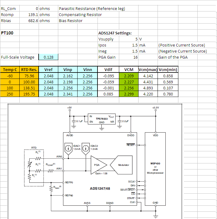
For the specified temperature ranges, resistance of RDT is 75.96 and 195.575 ohms. I am using compensations resistance as 139.1 @ 100dec C. I have calculated my R BIAS as 682.666ohms. Using these I am trying to calculate my DM and CM input ranges for a gain 0f 16 and I ref of 1.5mA. I am little bit confused about the results.

I am using the following application notes, which explains about 3-wire hardware compensation application.

http://www.ti.com/general/docs/lit/getliterature.tsp?literatureNumber=sbaa180&fileType=pdf

I have calculated the following:

                 DIF               CM

250C    0.0847V       2.3035V

-60C    -0.0947V      2.213V

From data sheet

AVSS + 0.1 + [(PGAGAIN)(VINdifferential)/2]  <   VCM   <   AVDD - 0.1 - [(PGAGAIN)(VINdifferential)/2]

AVSS = 0 , AVDD = 5V

by using this I calculated the allowable CM range,

0.167 < VCM < 4.8324 @ 250C   -0.6576 < VCM < 5.6576 @ -60C 

Can you explain me what these values are and what changes I have to make inorder to satisify CMm and DM ranges.

  • Hi Satya,

    Common Mode Voltage:

    Essentially both inputs of the ADS1148 device must be more than 0.1V away from the rails, and the equation below sets the common-mode voltage range limits for the internal PGA to work in its linear region.  When using the equation above with negative differential voltages, it is necessary to take the absolute value of the VINdifferential before inserting the value on the equation; otherwise the equation will not provide limits that make sense:

      AVSS + 0.1 + [(PGAGAIN)( |VINdifferential| )/2]  <   VCM   <   AVDD - 0.1 - [(PGAGAIN)( |VINdifferential| )/2]

    where VCM =(AINP+AINN)/2 and VINdifferential=AINP-AINN

    Provided that the calculated common-mode voltage on the RTD across temperature is inside the range delimited by the equation above, the PGA will be in its linear region.

    Full Scale Voltage:

    The Full-scale voltage of the converter is a function of the reference voltage, and PGA gain setting where:

    Full-Scale Voltage = +/-VREF/PGA;

    where the expected differential voltage should not exceed the full-scale voltage, and the user should select the PGA gain and IDAC settings accordingly

    According to the description above, the following settings are being used:

    IDAC1=1.500mA, IDAC2=1.500mA, RCOMP= 139.1 Ohm; RBIAS = 682.6; VREF=~2.048V and PGA=16

    Using the equations above, the VCM and VIN differential voltage is calculated across the temperature range; and provided that the VCM is in the allowed range; the PGA will be in its linear region.

    Using your example with the settings above, the calculations below were made; when using PGA=16 the device is inside its allowed linear region.  Please see the detailed calculations below.  Notice the differential voltage does not exceed the allowed full-scale voltage and the common mode voltage is inside the allowed limits across the RTD values over temperature.

    Best Regards,

    Luis


  • Thank you Luis. This really helped.