This thread has been locked.

If you have a related question, please click the "Ask a related question" button in the top right corner. The newly created question will be automatically linked to this question.

ADC122S625 - documentation issues

Other Parts Discussed in Thread: ADC122S625

Good morning,

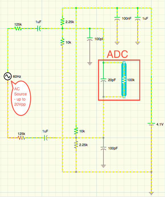
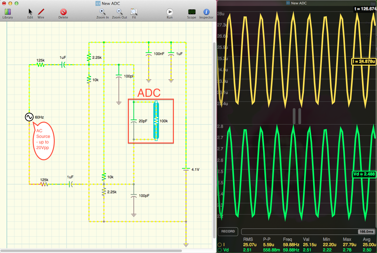
I wonder if someone can help me with this National Semi legacy ADC. The documentation is a bit too sparse for me, I apologize in advance! I am trying to use this ADC with an Arduino/Atmel microprocessor to sample voltage and current data concurrently, i.e. minimize phase lag between the two signals. I am using the two inputs in unipolar mode, as the current sensor has a 2.5V +/-2.0V output and the voltage transformer signal has been conditioned to be positive only also. 

1) What SPI mode should my micro-controller be using with this device? Reading the documentation suggests Mode0. 

2) The documentation re: the clock speeds on this chip is inconsistent. The eval board suggests a minimum clock speed of 6.4MHz for the on-board oscillator, the actual data sheet for the chip lists a maximum clock speed of 6.4MHz. I presume that there is no clock divisor on the board (that I could see), so what speeds should I be using? I am currently using the default 4MHz, though the Atmel can also go to 8MHz.

Thanks in advance, Constantin

  • Hi Constantin,

    Re 1: I am no expert on ATMEL processors, but looking at their APP note AVR151 the MODE 0 ought to work for you. The important thing here is to make sure that you are "sampling" DOUT with the rising edge of the SCLK

    Re 2: The MAX SCLK frequency is 6.4MHz

    Regards,

    tom

  • Hi Tom,

    Thanks for the response! With this chip I have also learned the importance of a very good voltage reference... now I use series references... 

    Does TI have any online references re: best practices on how to best hook up a differential inputs like the ones found on this chip to an AC source like the legs on a voltage transformer? I currently transmorgify this AC voltage signal into unipolar mode. However, it would appear that using the inputs in differential mode would be better, i.e. I would not lose a bit of resolution in the proces.. 

    Many thanks again, Constantin

  • Hi Tom,

    Thanks again for the help.  I have since found the TI guide to buffering, which can be found here: http://www.ti.com/lit/an/sloa098/sloa098.pdf. I am following in the footsteps of example 3.6, i.e. figure 7. However, I do not think I need a buffer, I am merely sampling a 60 Hz signal.  So this is the circuit I propose instead for the ADC122S625. The common mode signal is generated via a 4.096V series reference, the drop-down resistors hence bias the signal to be centered around 2.5V. 

    My question though is how to best model the ADC during operation? There is no mention of input impedance, just that the tracking cap is around 20pF. Is a 100K resistor assumption about right? Also, does this look like a proper differential input for the ADC122S625? Again, many thanks for your past help!

    Constantin

  • Hi Constantin,

    Sorry for the delay, but I am back :)

    What you are showing will impose a large DC potential (about 2.5V) across the ADC inputs. That, in my mind, is a waste of dynamic range as far as your signal is concerned. You may want to bias both inputs at 2.05V.

    Also, you signal will suffer a lot of attenuation on the way to the ADC input....

    I am sure you can work out the details.

    I am attaching a simple equivalent circuit of the ADC - at least as far as your input source is concerned.

    Regards,

    tom